Brigham Russell Frandsen and Dr. Bret C Hess, Physics and Astronomy
The area of nanoelectronic devices is a rapidly growing field as new devices and techniques are continually developed. This is an important field because it is hoped that devices of this scale will replace the current larger counterparts on computer microprocessors and other components, thus greatly reducing the size, and increasing the capabilities of computers.
The increased attention given to nanometer scale devices both in academic research and in industrial application has emphasized the importance of understanding the properties and behaviors of semiconductor nanocrystal electronic devices, and in particular the behavior of individual nanocrystals. The transport properties of many nanocrystal-based devices under ambient conditions are well characterized, or are in the process of being investigated, but the properties these same devices exhibit while subject to varying frequencies and intensities of illumination are not as well known. The properties of junctions involving one or a few nanocrystals are also not as completely understood.
The first task at hand to investigate the properties of nanocrystals was to determine and create a suitable electrical junction across which to measure the conductance through the nanocrystals. The chief difficulty in this arises from the extremely small size of the nanocrystals (~1-10nm), and because my goal was to investigate a junction involving one or a few nanocrystals, mechanical stability was of utmost importance. The technique I decided on and commenced implementing is the mechanically controllable break-junction (MCB) technique, only fairly recently developed. The advantages in using the MCB technique in investigating nanocrystal junctions are exceptional mechanical stability, and the ability to very precisely control the distance between the contacts of the junction.
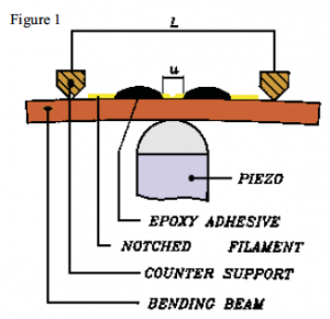
Designing, building, and implementing the MCB system has been the principal effort in my research so far, and indeed perhaps the name of the project should be changed to “Design and Implementation of Mechanically Controllable Break-junction Technique”, as much of the application and investigation of nanocrystal device transport is still to come. A schematic of the basic design principles behind the MCB can be seen in Figure 1 at left. The main elements in an MCB are the bending stage, onto which the sample (in my case a notched 100 micron gold wire) is mounted, counter supports (about 20mm apart) and a piezoelectric stack that provides the actual bending force. A piezoelectric stack is a device that elongates as a voltage is applied to it, exerting a force. The MCB can be used to investigate conductance across a junction by using the piezoelectric stack to bend the stage and break the gold wire at the point of the notching. By adjusting the voltage to the piezoelectric, the distance between the gold contacts (the broken ends of the wire) can be very precisely controlled, and contact can be broken or regained at will.
Because the MCB technique is still relatively new, ready-to-use commercial systems are not available, and the system had to be built from “scratch” so to speak. After designing and drafting schematics for all the parts I would need to build both the system and housing, I machined the components from aluminum stock and assembled the device. In my first setup, I used glass slides as the bending stage, because of their convenient size, electrical insulation, and ease of bonding to other substances. However, I soon found that even after notching and attaching the gold wire to the slide, the degree of bending required to break the wire far exceeded the limits of the glass, and the only result was broken slides.
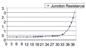
My next, and more successful design change was to use phosphor bronze instead of glass for the bending stage. Phosphor bronze is very commonly used in springs because of its flexibility and strength, and thus was a good candidate for a bending stage. I used thin sheets cut to approximately the same dimensions as the glass slides. To electrically insulate the stage from the gold wire, I used a thin film of epoxy. With this change, the MCB was successful; the wire was broken by bending the stage, and the contact distance could be controlled by varying the voltage to the piezoelectric stack. Contact breakage and distance was measured by finding the resistance across the junction. A low resistance (on the order of 1Ù) indicates the wire has not broken, while infinite resistance indicates that the wire has broken. By varying the distance, different resistances can be achieved. The figure to the left shows a curve typical to those achieved while testing the system. As the voltage to the piezoelectric increased (the x-axis), the resistance measured across the junction increased (y-axis).
The next step in building the system was to develop a computer interface the control the MCB and take data very quickly. To do this I designed a circuit using an operational amplifier to amplify the 10V that the computer’s A/D board could put out to the 100V that the piezoelectric required. Using the LabVIEW programming interface, I am able to control and take data from all of the instruments in the system, as well as control the MCB itself.
A functioning MCB system has been the biggest success of my research so far. However, there is still a great deal of work to be done, both in fine tuning the system, and in expanding its application. I would like to improve the system itself by achieving greater mechanical stability and reproducibility. Still to come as well is continuing to apply the MCB technique to investigating the transport properties of specific nanocrystals, and determining the feasibility of using these nanocrystals in devices on potential nano-scale computer chips.


