Jed Whittaker and Dr. Robert Davis, Physics and Astronomy
Atomic force microscopy (AFM) is a useful method for obtaining images of surfaces on the nanometer scale. It has been used to image surfaces in many environments, including in atmosphere, vacuum and fluids. The resolution of these images is subject to the size of the probe tip, which is pyramidal. It has been shown that the attachment of a carbon nanotube to an AFM probe tip increases resolution significantly, in both air and fluids1. The nanotubes have initially been attached by Van der Waals forces, individually, which are too weak for applications in fluids. For use in fluids, glues and coatings have been painstakingly applied to individual nanotube tips. Also, beyond fluids, low-temperature/high-vacuum applications would require a more rigidly attached nanotube than Van der Waals forces can provide.
Another issue that arises with electrostaticaly-attached nanotubes is their length. They tend to be hundreds of nanometers long, with aspect ratios too large for the high-resolution images possible with short tubes. For AFM probes with nanotube tips, a tube shortening method is desirable. Previous attempts have been mechanical, such as hitting the tube on the surface until it slides up the probe tip, or electrical, like applying a short voltage pulse across the tip to break the tube. Both have experienced marginal success. The major problem with all attachment and shortening methods to date is that they require individual manipulation of nanotubes and probes, which is costly, time-consuming and has limited reproducibility.
I proposed to develop a method of attachment using a silicon dioxide thin film to selectively coat the nanotube and probe tip. The selectivity to not coat the nanotube where it does not touch the silicon substrate has already been shown2. After deposition, the exposed tube section was to be removed and a small amount of the deposited oxide was to be etched back, exposing a short section of nanotube for imaging. This method has the potential to revolutionize high resolution AFM by providing reproducible and cost-effective rigid attachment and shortening.
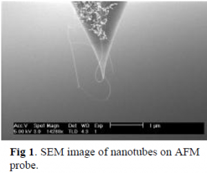
The nanotubes were commercially grown off the AFM probe tip by chemical vapor deposition (CVD) from a common alumina-supported solution catalyst, which consistently yields single walled nanotubes 1-2 nm in diameter. This process has been used for few years now, and the nanotube AFM probes were made by NanoDevices. Nanotube probe tips were confirmed by scanning electron microscopy (SEM) to have a nanotube growing off their end (Figure 1). The nanotube AFM probes were placed in a specially constructed CVD chamber, containing two independently controlled heaters. In this chamber, silicon tetraacetate was heated to 100ºC, just below its melting point. The probe tip was held 1-2 cm from the silicon tetraacetate and heated to 170ºC. It has been shown that silicon tetraacetate will decompose to silicon dioxide and a vapor phase acid anhydride at 160 to 170ºC3. The chamber was held under vacuum at a pressure of a few Torr.
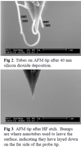
After silicon dioxide deposition (Figure 2), the nanotube diameters were measured by SEM and compared to previous measurements. The tube diameters increased from 8 nm before deposition to 87 nm after deposition, indicating that a 40 nm film had been deposited. For an unexplained reason, selectivity had not been achieved, so an alternate method was tried. To expose the nanotube tip, it was immersed in a 10:1 buffered hydrofluoric acid solution for 20 min, assuming an etch rate of 1 nm/min, to etch back half of the oxide. It has been previously shown that hydrofluoric acid will not damage carbon nanotubes, while still etching silicon dioxide. This selective etch allowed for the nanotube to be exposed, but SEM (Figure 3) showed that something in the liquid etch, probably surface tension, had forced the tube to lay down against the left side of the AFM probe. This is evident from the bumps on the pyramid edge where the nanotube originally left the surface.
This method has not yet been successful in producing a functional AFM probe, but still holds promise. The silicon dioxide deposition parameters need to be adjusted to be selective to the silicon surface and not deposit on the protruding nanotube. This would allow tube shortening before the wet etch, overcoming problems with surface tension.
Successful application of this method will allow for large scale, consistent production of shortened, rigidly attached carbon nanotube AFM probe tips. They would find applications in areas such as condensed matter physics, zoology and materials science.
References
- J. H. Hafner, C.-L. Cheung, T. H. Oosterkamp, C. M. Lieber, J. Phys. Chem. B 105, 743 (2001).
- J. D. Whittaker, M. Brink, G. A. Husseini, M. R. Linford, and R. C. Davis. Submitted to Applied Physics Letters, March 2003.
- T. Maruyama, J. Shionoya; Jpn. J. Appl. Phys. 28, L2253 (1989).


