
Jorj Ian Owen and Dr. Robert C. Davis, Physics and Astronomy
Introduction and Background
A light emitting diode (LED) is a semiconductor device that gives off light. An LED works by the combination of electrons and electron holes (a moving, positive charge caused by missing electrons). As the electron and electron hole combine, the electron joins the atom in an excited state (some greater than minimum energy level). The high-energy electron will then decay into a lower energy state by emitting a photon, a packet of energy. LEDs are useful for many reasons. For example, they are extremely efficient in converting electricity into light (unlike conventional tungsten bulbs), they do not get very hot, and the light produced is all of a similar wavelength and can be used for making displays.
Most LEDs currently in use are made by doping polymers (a process of making plastic, normally an insulator, into a semiconductor), or at an interface of gallium and arsenide-phosphide. These methods have allowed the invention of only a handful of LED colors.
Research Project
Over the past year we have been working on creating a new type of LED consisting of cadmiumselenium (CdSe) nanocrystals sandwiched between polyelectrolyte multilayers. A nanocrystal is exactly what the name implies: a very small crystal. Nanocrystals act like a quantum-mechanical “particle in a box”: they have the useful property that the color of the light they emit depends solely upon their size. Nanocrystals can be fabricated in a wide range of sizes. Therefore, if this process was perfected, an LED of any color could be made.
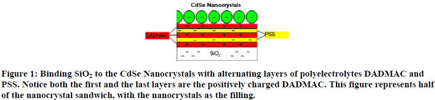
Polyelectrolytes are long polymer chains that have a positive or negative charge. Alternating layers of positively and negatively charged polyelectrolytes accomplishes two major objectives. First, they provide a way to bond silicon-dioxide (SiO2) to the nanocrystals, both of which have a residual negative charge (see figure 1). Second, applying alternating layers of polyelectrolytes to the SiO2 creates energy gaps. These energy gaps produce the energy difference that allows the electrons and electron holes to recombine and emit light. The energy difference required for every size nanocrystal is different, so the thickness and number of layers of polyelectrolytes will need to vary depending on the nanocrystal size.
Steps Toward Creating a Nanocrystal LED
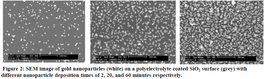
Making a preliminary sample- By laying down polyelectrolyte multilayers on a silicon wafer followed by gold nanoparticle deposition on top, we made a preliminary sample that would not emit light, but did tell us that this bonding method is viable. We obtained images of the samples using a Scanning Electron Microscope (SEM), see figure 2.
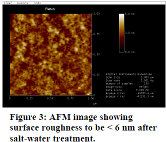
Flattening the polyelectrolyte layers- If the layers of polyelectrolytes are not even, then not as many nanocrystals will glow. Using an Atomic Force Microscope (AFM) we looked at the layers, and found them not to be very even (> 20nm variation). By dipping the samples in salt water the variation over the surface was lessened (< 6nm), see figure 3.
Finding the I-V curves- We are focusing our research on two methods of finding out how the current through the polyelectrolytes varies with the thickness of the layers. One way is to deposit the polyelectrolytes on gold, then deposit another layer of gold on top. By changing the voltage across the sample we can find how the current varies, see figure 4a. The second method is to create a grid of small wires via electron beam lithography, then deposit the polyelectrolytes, and finally measure the current between small gaps in the wires as voltage is varied, see figure 4b.
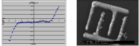 Figure 4: Two methods of finding I-V curves (a) Measurement of polyelectrolytes sandwiched between gold layers. (b) SEM image of ~30 nm wires made by electron beam lithography.
We hope eventually to match a particular thickness of polyelectrolyte multilayer to a particular size nanocrystal. We anticipate this method to enable the production of light of almost any color.