Daniel W. Pulsipher and Dr. Craig Petrie, Electrical and Computer Engineering
Analog-to-digital converters (ADCs) play a prominent role in modern electrical systems. The environment in which we live consists primarily of analog signals, information-carrying waveforms continuous in time and value. Because of this continuous characteristic, analog signals are difficult to store and manipulate. Digital signals are sampled in time and quantized (rounded) in value. Processing of a digital signal can be done more efficiently and flexibly than processing of an analog signal. ADCs are universally needed to construct high-performance digital electronic systems such as cellular phones, satellite equipment, medical instruments, and electronic sensors.
The flash ADC is the most basic but most widely used ADC architecture. Many more complex ADC architectures such as pipelined, two-step, and sigma-delta ADCs incorporate flash ADCs as internal sub-quantizers. A flash ADC consists of a resistive voltage divider (“resistor string”) connected to a bank of comparators. A comparator produces a digital “1” when its input voltage is positive; otherwise it produces a digital “0”. The comparators are arranged so that N uniformly-spaced reference voltages are compared in parallel to a single input voltage, vin. An encoder translates the N one-bit digital signals to a single log2(N)-bit digital output code.
An ADC must encode its analog input as accurately as possible. As the clock signal is applied to the comparator in a flash ADC, it dynamically couples onto the resistor string. This coupling distorts the reference voltages and causes inaccurate conversion. The resistor values may be lowered in order to decrease coupling of the clock signal. However, as the resistor values are lowered, an increase in current is necessary to maintain the proper reference voltages; this increases the power consumption of the overall ADC.
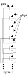
In the first attempt to design a reference string, PMOS transistors were used in place of the resistors (see figure 1). Using the PMOS transistor would decrease both the power consumption and the coupling effect. The main challenge in using this method was turning the transistors “on”. In order for this to happen, the transistor gate voltage has to be lower than the threshold voltage. This would be accomplished in this design by connecting the gate voltage to the voltage three or four taps down from the transistor. Once all the transistors were “on” all taps would be identical and therefore the reference voltages would be correct.
Once the idea for the design was completed I built a model circuit using Cadence. Upon simulating the circuit a problem was discovered. The bottom of the reference string was causing residual effects throughout the rest of the string. Extra taps had to be added on the bottom of the string beyond the N taps used for the reference voltages. This would allow for the lower reference transistors to be turned on. However, even with the extra transistors and adding a current source the other transistors on the string were not all identical and therefore would not produce accurate results.
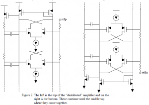
Eventually it was decided that instead of pursuing the first design further a new design would be designed and tested. This design would attempt to take advantage of the properties of a feedback amplifier. A feedback amplifier has two inputs, an output and feedback from the output to one of the inputs. The amplifier forces the two inputs to the same voltage. When the amplifier input that connects to the input of the comparator is changed the feedback from the amplifier forces it back to the voltage of the other input which is connected to a resistor reference string. In order to minimize gates and area on the circuit die the design was implemented using a “distributed” amplifier design. (see figure 2)
This design was analyzed and then a model was built using Cadence. A simulation was performed by applying a current pulse to each of the inputs. The transient response of the inputs was then analyzed. The ideal behavior would be a drop in voltage and then a return to the correct reference voltage. Unfortunately, when the simulation was run the results were not in accordance with what was expected. The current pulse caused the circuit to oscillate and not return to a stable state. When an amplifier is not stable this oscillating effect sometimes occurs. The next step in the process is to analyze and test the stability of each small piece of the distributed amplifier.
I am now in the process of working with one of Dr. Petrie’s graduate students in testing the stability of the amplifier. Once the amplifier is stabilized further simulation will be performed and the results analyzed to verify that the circuit functions as expected.


