Stephen Markham and Dr. Aaron Hawkins, Electrical and Computer Engineering
Abstract: Waveguides will become more important as optical networks replace traditional wire networks for data transfer. This research explores one method of creating multimode waveguide that uses Plasma Enhanced Chemical Vapor Deposition to grow oxide and nitride layers on Silicon.
As the Information Age matures, society has ever expanding needs for high speed communication. Optical networks are capable of extremely high rates of data transfer computer to traditional copper wire based networks, and are continually being implemented in greater numbers throughout the world. Traditional networks use integrated circuits to process and control the flow of information. Optical network rely on waveguides to perform this task. The industry standard for producing multi-channel waveguides requires accurate Silicon Oxide and Silicon Nitride deposition. In this research deposition of these materials is explored using a PECVD machine.
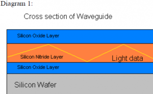
To understand how a waveguide works, it is best to think of light bouncing between two mirrors. If the two mirrors run parallel to each other the light will stay between them, even if they bend, curve, or continue for a long distance. Even if the light is not aimed directly between the mirrors, it will bounce back and forth between them, always moving towards its final destination. To create two parallel mirrors, a layer of silicon nitride is sandwiched between two silicon oxide layers. The light travels through the silicon oxide, which has an index of refraction1 of about 1.45, and reflects back into the oxide when it hits the nitride layers, which have indexes of refraction of about 2.02.
The amount of light reflected back into the middle of the waveguide depends on the wavelength of the light, the thickness of the layers, and the index of refraction of each layer. By controlling the thicknesses of the layers very accurately, and by adjusting the indexes of refraction, the mirroring effect is increased, and less light is lost through the nitride layer. This research characterized the growth rates and indexes of refraction of oxide and nitride layers when they were deposited using a PECVD machine.
Plasma Enhanced Chemical Vapor Deposition is a fascinating method for growing oxide and nitride on silicon wafers. First, the silicon wafer is placed on a plate that is heated to 300 degrees Celsius. Then plate and wafer and sealed in a chamber which is then vacuumed down to very low pressure, about 50 milliTorr3, so that the wafer is not exposed to impurities in the air. Nitrogen, a non-reactive gas, is introduced at a pressure of about 1 Torr. Next, other gases are introduced to form the material to be deposited. For example, to produce an oxide layer, silane, SiH4, and nitrous oxide, NO, are introduced into the chamber. These react to form SiO2, silicon dioxide. For a nitride layer, ammonia, NH4, is substituted for NO, to form SiOxNy. Note that the nitride is not stoichiometric—the ratio of oxygen to nitrogen is not always the same. To control the amount of nitrogen in the compound, and thereby control the index of refraction, different ratios of gases are introduced into the chamber.
This research was concerned mainly with two things: characterizing the PECVD machine recently acquired by BYU’s Integrated Microelectronics Laboratory (IML), and to determine recipes for oxide and nitride layers of various indexes of refraction and growth rates. While there are accepted values for the indexes of refraction of both oxide and nitride layers, this research found recipes that would produce other values as well. In all cases, the recipe that produced a given layer at a certain index of refraction with the fastest growth rate was considered the best recipe.
While growth rates and indexes of refraction followed some general trends, it was still necessary to grow many recipes to record their growth rates. The findings of the research are, unfortunately, unique to the specific PECVD machine in BYU’s IML, and cannot be generalized to other laboratories because of peculiarities inherit in a custom built machine. However, the results for that single machine are consistent, and serve as a valuable resource for researchers currently working on a new type of waveguide involving many alternating layers of oxide and nitride.
The research was successful in characterizing the PECVD machine, and in finding a useful oxide deposition recipe. Unfortunately, the nitride deposition did not go as well, and no single recipe came forth as the best. In order to control the index of refraction, the strength of the nitride must be sacrificed. This research is currently being extended to continue searching for a strong nitride with the desired index of refraction of 2.0. For a current description of recipes research results so far, please visit http://www.ee.byu.edu/cleanroom/pecvd.phtml.

