John Wilcox and Dr. Robert Davis, Physics and Astronomy
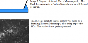
BYU’s Nanotube Research Group is currently searching for a method to attach and shorten carbon nanotubes (CNTs) on the tips of Atomic Force Microscope (AFM) probes (image 1). Many have shown that short CNTs grown on the end of AFM probes greatly enhance the resolution and utility of the AFM. With shortened CNTs securely attached to the tip of an AFM probe, the microscope resolution could be improved as much as 5 times. It has been shown that features as small as 1.5nm can be measured . CNTs are strong and have small diameters which make them ideal for scanning probe microscopes .
The method being developed here at BYU can be applied to mass fabrication and provide AFM researchers everywhere with durable high resolution CNT probe tips. In my project I tested the selectivity of SiO2 by attempting to deposit SiO2 on graphite sheets from a silicon tetraacetate precursor. BYU researchers have been able to grow and securely attach CNTs to substrates by depositing SiO2 over the tubes from a silicon tetraacetate precursor. During their experiment they were unable to directly show with chemical analysis that SiO2 did not deposit on the CNT itself. This deposition selectivity is crucial to the CNT probe fabrication technique.
Graphite has very similar molecular and chemical properties to CNTs. CNTs are rolled up graphite sheets and therefore retain similar surface properties of graphite. We expect that the SiO2 will not deposit on the graphite surface because of chemical incompatibility between the graphite and silicon tetraacetate.
First, I grew SiO2 in a vacuum chamber on a silicon surface and then measured the growth to verify that SiO2 was deposited on the silicon. This was done in a vacuum chamber by heating a small amount of silicon tetraacetate, under the sample. Next, I attempted to grow a SiO2 layer on a graphite substrate and silicon surface at the same time, using the same method. The silicon was the control.
I measured the amount of SiO2 on the silicon chip using an Ellipsometer to verify that SiO2 was deposited on the control piece of silicon. I exposed the graphite sample to Si and O2 and gave them a chance to deposit SiO2 on the graphite surface.
During the exposure, 30ns of SiO2 was deposited on the silicon sample. I then measured the graphite sample using the X-ray detector on the JEOL Scanning Electron Microscope. The SEM showed that the amount of X-rays for silicon on the graphite sample was barely above background noise (image 2). From the number of X-rays I detected, I concluded that there was only a small amount of Si02 on the graphite.
Next, I measured the graphite sample using the X-Ray Photoelectron Spectroscopy (XPS). The XPS measured the surface of the graphite to be 6% Silicon. This means that approximately 5 nanometers were deposited on the graphite, which is 6 times less than the SiO2 deposited on the silicon wafer.
From the measurements that we have taken there was a very small amount of SiO2 that may have been deposited on the graphite. Because the surface of the graphite sample was not one continuous sheet as seen in Image 2, the SiO2 may have bonded to the edges of planner surfaces and on other debris on the surface . This would explain why less was deposited on the graphite sample. We have determined other ways to test this sample that may reveal the surface structure a little better. We are also going to study more closely the temperatures and pressures at which the deposition is preformed to see if there is an ideal temperature and pressure at which the SiO2 grows less on the graphite.

References
- Stanislaus S. Wong, Adam T. Woolley, Teri Wang Odom, Jin-Lin Huang, Philip Kim, Dimitri V. Vezenov, and Charles M. Lieber, ” Single-walled carbon nanotube probes for high-resolution nanostructure imaging” Applied Physics Letters Volume 73, Issue 23, pp. 3465-3467 (1998).
- Jason H. Hafner, Chin Li Cheung & Charles M. Lieber. 1999 Growth of nanotubes for probe microscopy tips. Nature 398, 761 – 762.
