Randall Stoltenberg and Dr. Adam T. Woolley, Department of Chemistry and Biochemistry
ABSTRACT
DNA-templated nanofabrication is a promising route toward miniaturization of electronic devices below the 100 nm range. We have developed methods for fabricating micrometer-length copper nanostructures with nanometer heights from DNA templates on silicon surfaces. These structures have been integrated into simple circuits for electrical characterization. Atomic force microscopy and transmission electron microscopy suggest that these constructs are composed of copper metal. However, copper metal was not detected by scanning electron microscopy analysis. The present structures have resistances in the TΩ range or higher, and approaches for achieving improved conductivity are presented.
INTRODUCTION
Miniaturization of electronic devices into the nanometer range presents formidable obstacles to conventional microfabrication techniques. Alternatively, bottom-up self-assembly entails constructing electronic components from their atomic and molecular building blocks. Thus, it may be feasible to fabricate nanometer-scale devices without using cleanroom facilities.
Metallic nanowires have been fabricated using bottom-up self-assembly, in particular through the use of biotemplates such as DNA to enable controlled growth and localization. Employing DNA as a template yields further advantages in device construction. DNA acts as a general template for metal deposition, and the specific molecular recognition of base sequences can be exploited to address electronic components. Varying approaches to nanowire fabrication have been proposed, yet these methods require extensive optimization for nanoelectronic applications.
We are studying the metallization of surface-adsorbed DNA to produce conductive DNA-templated copper nanowires. Copper-metallized DNA has been reported, , , but electrical characterization of these constructs has not. Herein, we describe methods for copper nanowire fabrication as well as techniques for integrating these structures into circuits for electrical characterization. The reported nanostructures have been studied by atomic force microscopy (AFM), scanning electron microscopy (SEM) and low-current four-point microprobe parametric analysis.
EXPERIMENTAL
Elongated, surface-adsorbed DNA (New England Biolabs) was prepared by translation of small droplets (~1 L) of dilute DNA solution (1–50 ng/L) across a clean silicon substrate. Oxidized silicon surfaces were pretreated with a 1 ppm solution of poly-L-lysine (Ted Pella, Inc.) for 5 min to render the surface positively charged for optimal DNA adsorption. Adequate DNA coverage of the surface was achieved using 2–10 ng/L DNA solutions. Silanized silicon surfaces were prepared by placing ~30 mg of chlorodimethyloctadecylsilane (95%, Aldrich) on the heated surface of an oxidized silicon wafer, which had been cleaned previously in concentrated sulfuric acid, rinsed with water, and then dried at 110 ºC. After 20 min, the excess silane was removed by rinsing with copious amounts of acetone and isopropanol. For these surfaces, no poly-L-lysine treatment was necessary, and adequate DNA coverage required DNA solutions of 20–50 ng/L.
Surface-adsorbed DNA was incubated in 40 L of 0.5 M Cu(NO3)2 (Mallinckrodt) in dry dimethylsulfoxide (DMSO, EMD) for 20 min. To this solution was added 40 L of 1 M aqueous ascorbic acid (Sigma), and the combined solution was allowed to react for 4 min. Next, the surface was rinsed with deionized water and dried with compressed air. Electroless plating for additional copper metallization was carried out in 2 g/L cupric nitrate (Mallinckrodt), 30 g/L sodium potassium tartrate (Mallinckrodt), and 10 g/L NaOH (Spectrum) in 1.4% aqueous formaldehyde (Mallinckrodt). The recommended temperature and incubation time for this electroless plating system are 35 ºC and 15 min, respectively. However, plating at this temperature was detrimental to the surface-adsorbed DNA, so experiments were conducted at room temperature.
Gold electrodes were deposited on the surface of oxidized silicon wafers by conventional lithographic techniques. The electrodes were separated by ~8 m to ensure that single DNA molecules (~16 m length) could contact adjacent electrodes (Figure 1). Conductivity of the resulting nanostructures was measured by low-current four-point microprobe analysis using a computer interfaced with a two channel parametric test system (Agilent E5262A). Voltage was swept from -40V to +40 V to generate a current vs. voltage curve from which the resistance of the system was calculated.
AFM images were captured using a Digital Instruments Multimode instrument in tapping mode. Tips had resonant frequencies between 55–75 kHz. SEM analyses were conducted using a Philips XL30 ESEM FEG system with 5.0 and 10.0 kV beams.
RESULTS & DISCUSSION
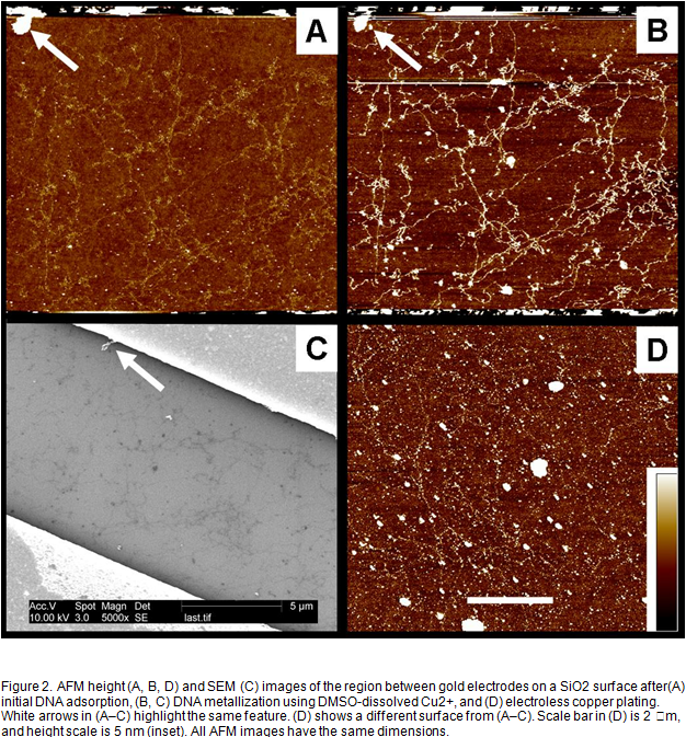
SiO2 Surfaces. Previous studies of copper-metallized DNA showed that surface-adsorbed DNA was readily cleaved after one or more treatments with aqueous copper solution,2 a result ascribed to hydroxyl radical formation in the presence of copper ions. This DNA fragmentation has been reduced by dissolving Cu2+ in DMSO. Copper deposition after one metallization treatment was not continuous but resulted in an average height increase of 1 nm (Figure 2A-B). Additional electroless plating at room temperature has not been successful to date in increasing wire height or continuity. In some instances, the height of the original copper nanostructures decreased after electroless plating (Figure 2D). This is possibly due to the tartrate, which decreases the reduction potential for deposited copper metal on the surface, leading to increased copper metal oxidation and dissolution. Also, the extent of non-specific copper deposition appeared to increase after electroless plating. Performing the plating reaction at 35 ºC caused the surface-adsorbed DNA to be fragmented and desorbed.
SEM images of these DNA-templated structures did not show copper X-ray signals. Two factors may explain this result. First, the resolution of the SEM (>5 nm) could be insufficient to detect copper nanostructures only ~1 nm in diameter. However, transmission electron microscopy (TEM) images of surface-adsorbed DNAs show that the molecules are plated by copper metal after one metallization treatment. Alternatively, the apparent height increase in AFM may be due to salts adsorbed to the DNA, a scenario consistent with the Na X-ray signal detected in large-field SEM scans.
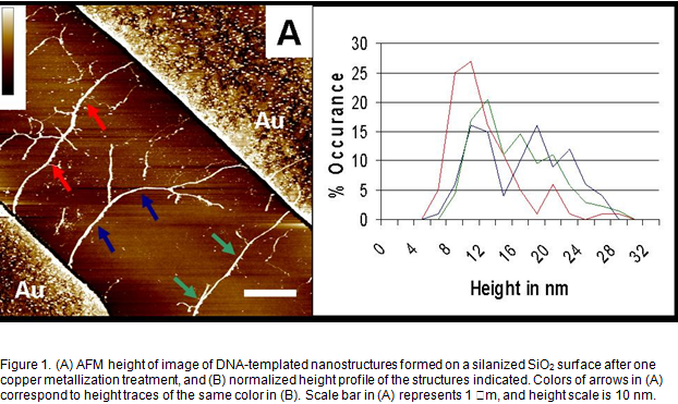
Silanized Surfaces. Silane-treated SiO2 surfaces at first appeared to be advantageous relative to poly-L-lysine-treated oxide surfaces, as nonspecific copper deposition was reduced without a need for surface masking techniques.3 DNA bundling was a significant down-side to using these substrates, but the bundle dimensions increased more than single molecules after one metallization treatment. AFM data indicated that nanostructures formed after one metallization treatment had an average height of 12 nm and bridged the gold electrodes (Figure 1A). However, no conductivity was measured through these nanostructures, and no copper signal was detected in SEM.
Conductivity Measurements. Parametric analysis of nanostructures formed on either silanized or poly-L-lysine-treated SiO2 surfaces showed these constructs to have resistances in the TΩ range or higher. Possible reasons for the high measured resistance include poor DNA-electrode contact, insufficient copper metallization, wire discontinuities, and oxidation of copper metal in air. The issue of poor contact can be addressed by two procedures. First, thiol-modified oligonucleotides complimentary to the “sticky” ends of DNA will be adsorbed on the gold electrodes to increase the probability of single molecules spanning adjacent electrodes. Second, the contact between the nanowires and the electrodes can be improved by depositing a carbon film over the contact interface by SEM. Optimization of both the initial copper deposition and electroless plating procedures should improve wire continuity and increase wire diameter. Copper oxidation can be prevented by fabricating the devices in an inert atmosphere, or oxidized structures can be reduced by annealing the wires in H2¬. Implementing these improvements should yield conductive copper nanostructures on surfaces to allow electrical characterization by four-point microprobe parametric analysis. These integrated nanostructures should be important components for DNA-templated nanoelectronics.
CONCLUSIONS
DNA-templated nanostructures formed on patterned silicon surfaces after copper metallization treatments yield high resistance networks. AFM images suggest these structures are taller than native surface-adsorbed DNA, but copper metal is not detected in SEM (although it has been observed in TEM). These data call for improved copper metallization and DNA surface adsorption techniques to produce conductive copper nanostructures. Thiol-modified oligonucleotides will fix DNA to gold electrodes, and SEM carbon deposition on nanowire-gold interfaces will decrease contact resistance. DNA-templated copper deposition will be augmented by refining the initial metallization treatment and the electroless plating conditions to suit this specific application. By optimizing these procedures, we should be able to construct conductive DNA-templated copper nanowires as a step toward bottom-up self-assembled nanoelectronic devices.
ACKNOWLEDGMENT
We acknowledge the Brigham Young University Microscopy Laboratory for SEM and TEM training and the following organizations and grants for funding: Brigham Young University Office of Research and Creative Activities, Environments for Mentoring Grant from Brigham Young University, the Petroleum Research Fund administered by the American Chemical Society, and the U.S . Army Research Laboratory and Research Office under grant number DAAD19-02-1-0353.
References
- Stoltenberg, R. M.; Woolley, A. T. Biomed. Microdev. 2004, 6, 105–111.
- Monson, C. F.; Woolley, A. T. Nano. Lett. 2003, 3, 359–363.
- Becerril, H. A.; Stoltenberg, R. M.; Monson, C. F.; Woolley, A. T. J. Mater. Chem. 2004, 14, 611–616.
- Becerril, H. A.; Stoltenberg, R. M.; Wheeler, D. R.; Davis, R. C.; Harb, J. N.; Woolley, A. T. J. Am. Chem. Soc. 2005, 127, 2828–2829.
- Electroplating and Electroless Plating of Copper and Its Alloys; Kanani, N., Ed.; ASM International: Materials Park, Ohio, 2003.
- Lamour, E.; Routier, S.; Bernier, J.-L.; Catteau, J.-P.; Bailly, C.; Vezin, H. J. Am. Chem. Soc. 1999, 121, 1862–1869