Shiul Khadka and Dr. Brian Mazzeo, Department of Electrical and Computer Engineering
Abstract
In this project, we developed a process to integrate microfluidic channels on standard radio- frequency (RF) A 10.56 GHz RF microstrip interferometer was fabricated using the proposed technique and used to compare electrical responses for liquids with various dielectric properties and thereby demonstrate the capability of RF PCB-integrated microfluidic devices for biological sensing. Microchannels were milled into a substrate and prepreg outlines for microchannels were cut using a laser system. Substrates were adhered and bonded by clamping and baking. The RF interferometer responded to changes in liquid permittivity with high sensitivity relative to many other types of dielectric sensors.
Introduction
Electrical interrogation in microfluidics has been explored extensively because of the advantages of using integrated, compact microelectronics to perform liquid sensing and control. The traditional fabrication route is to create an electrical network on one substrate and then use an elastomer or other thermoplastic to form fluid channels which are then adhered to the electrical network [1, 2]. Alternatively, liquid channels and the electrical network are formed by lithography, etching, and deposition processes performed in a cleanroom [3, 4]. These processes generally require materials and adhesives that are not found in traditional printed circuit board (PCB) fabrication processes. It would be advantageous to use tools and techniques that are already found in industry to fabricate microfluidics that can be incorporated simply with standard multi-laminate RF PCB processes for reduction in fabrication complexity, time, and cost. This would allow microfluidic devices to be fabricated by researchers without cleanrooms, and simplify the integration of commercial devices with RF interrogation electronics.
Fabrication
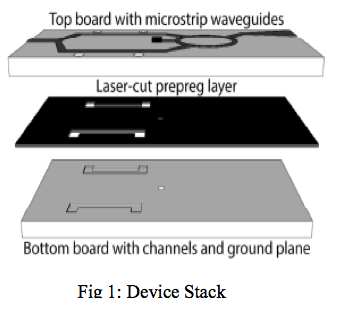
The main goal behind the ORCA proposal was to successfully fabricate microfluidic microstrip design of interferometric device. The fabrication was done successfully and the process is outlined here. The RF interferometer was fabricated using traditional PCB processes as shown in Fig. 1. The substrates were RO4003C board (Rogers Corp.) which has copper layers on both sides. The dimensions of the board were cut to 1 in. by 2 in. The top board which contains the RF waveguides was patterned using a FP-21T PCB Prototyping Machine (MITS Electronics). The copper was peeled from the underside of the board, removing the original ground plane. Access holes in the top substrate were drilled.
The copper layer was peeled from a second board of equal dimensions and then milled at a depth of 10 mils to form microchannels. RO4450F prepreg (Rogers Corp.) was then laser cut to the same size as the top and bottom boards and to remove areas corresponding to the microchannels using a Rayjet 50 C30 laser engraver (Trotec).
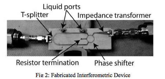
The two boards were then aligned with the microchannels on the inside and sandwiched together with the prepreg layer in between. The boards were clamped together between aluminum blocks and then baked at 210 °C for an hour in an oven (J. C. Penney Co., Inc. Model 4780/1) [13]. The prepreg sealed the boards and the microchannels. A photograph of the completed device is shown in Fig. 2. Flexible plastic tubing was attached with Loctite® Epoxy Marine (Henkel Corp.) for liquid introduction into the microchannels.
Experiment
The interferometer was placed in position and then connected to the network analyzer through SMA connectors. The untuned characteristics of the waveguide were recorded for further comparison with simulation. Tuning consisted of placing the plastic clamp appropriately so that the wave speed in the reference branch matched the test branch so that a significant transmission null was created. For liquid experiments, the waveguide was first tuned appropriately with air to generate a significant transmission null for the air matching condition before liquids were introduced. Fluids were inserted into the test channel using a syringe. Ten frequency sweeps were recorded for isopropyl alcohol, IPA (Sigma-Aldrich Product 190764, ≥99.5%) and de- ionized water from our BYU cleanroom.
Results and Conclusions
We have demonstrated fabrication of microfluidic channels in materials and processes consistent with RF PCB manufacturing processes. These channels were used as part of a liquid RF interferometer which was designed for 10 GHz, with an actual measured null frequency of 10.56 GHz. A sensitivity of approximately 13.6 dB/∆ε was thus demonstrated in this device for the measured difference between air and IPA. The procedure described here will allow other researchers to create microfluidic devices integrated with RF electronics. The RF waveguide structure itself was demonstrated to be a valuable general platform for measuring very small changes in dielectric properties of materials.
References
[1] J.C. McDonald, D.C. Duffy, J.R. Anderson, D.T. Chiu, H. Wu, O.J. Schueller, and G.M.Whitesides, Fabrication of microfluidic systems in poly(dimethylsiloxane). Electrophoresis 2000, 21 (1), 27-40
[2] K. Park, H.J. Suk, D. Akin, and R. Bashir, Dielectrophoresis-based cell manipulation using electrodes on a reusable printed circuit board. Lab On A Chip 2009, 9 (15), 2224-2229.
[3] T. Shang, E. Teng, A.T. Woolley, B.A. Mazzeo, S.M. Schultz, and A.R. Hawkins, Contactless conductivity detection of small ions in a surface micro-machined CE chip. Electrophoresis 2010, 31 (15), 2596-601
[4] J.R. Lee, J.P. Barber, Z.A. George, M.L. Lee, H. Schmidt, and A.R. Hawkins, Microchannels with rectangular and arched core shapes fabricated using sacrificial etching. Journal Of Micro- Nanolithography Mems And Moems 2007, 6 (1), 013010.


