Mallory Phillips and Dr. Aaron R. Hawkins, Electrical Engineering Dept
Optoelectronics are made on the surface of a thin substrate of semiconductor material by attaching light-sensitive polymers to the surface, then removing patterns generated in the polymer. Waveguides can be made on the same substrate to interface directly with optoelectronics. They are made from raised channels running along the substrates surface and guide light through total internal reflection, much like optical fibers [1]. Optical fibers are used for internet and cable connections, in order for information to be successfully used, that information must make a transition from the optical fiber to integrated waveguides [2]. The engineering challenge associated with this transition involves the precise placement of waveguides and fiber, which can require better than one micron precision. The purpose of this project was to create a coupler that would serve as a bridge to guide light from an optical fiber into a waveguide efficiently.
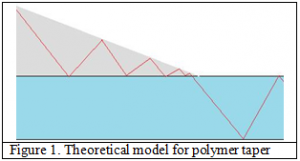
In practice, the coupler was to be formed by embedding an optical fiber in a polymer that is applied to the surface of a glass substrate. The polymer tapered from a thick section adjacent to the fiber into a thinner section on the substrates surface. Light moving through this taper would be “squeezed” into a smaller and smaller beam until it coupled into the on chip waveguide as illustrated in Figure 1.

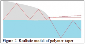
After creating this fabrication technique, the devices were tested by stripping the casing from the free end of the fiber. In early stages of testing, this free fiber end was spliced with a fiber that included at attachment. This attachment could be connected to a light source so that light was guided down the fiber and into the polymer. In this way red light could be seen, ideally, inside the glass slide. In reality, red light was seen coming out of the bottom and top of the slide, and most often light appeared to be coming out of the polymer ramp and skimming the top surface of the glass slide. By close inspection, it was determined that the linear ramp looked less like Figure 1 and more like Figure 2.

The ramp illustrated in Figure 2 was also found when the ramp was fabricated using the traditional method of spinning the polymer on the substrate. This shape proved to be a major problem in the success of this device. With my mentor, and other student collaborators, we could not find a way to overcome the tendency of polymers to create this shape no matter the thickness, or speed (ranging from gravity-fed method up to 6000 rpm on Soli-Tek spinner.)
This project evolved to a new project dealing with polymers treated through known lithography processes to create a linear ramp. This process is promising and will be an integral step in the creation of multi-step Nanosieves. Nanosieves consist of an array of micro channels with the purpose of separating biological material on the nano-scale according to size.
