Alan Nelson
In my ORCA grant proposal, I described a novel solid-state amplifier known as the SIM (Solidstate Impact-ionization Multiplier) that has been developed here at BYU. It is particularly useful for amplifying weak optical signals—weak such that they would require low-noise amplification in order to avoid garbling the signal with added amplifier noise. The mechanism driving amplification in the SIM—Impact-ionization—is inherently low noise. Due to it being relatively easy and inexpensive to manufacture the SIM (compared with other low-noise amplifiers such as the Avalanching photodiode), as well as many other benefits outlined in my proposal, the utility of enhancing the SIM is clearly evident.
One of the barriers preventing the SIM from being on-par with other low-noise amplifiers is its gain efficiency. This was the problem that I focused on in my research—creating a SIM that has higher, easier to control gains. My proposal was to alter the geometry of the SIM so as to result in more gain events. The desired result was to force the electrons through high electric field region in the device, resulting in an increase in impact-ionization events and thus an increase in gain efficiency.

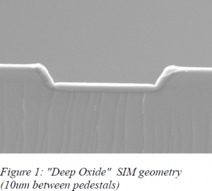
Because the high e-field region always shows up at the corner of the P-N junction between the input and output nodes, it made sense to create an insulating barrier in such a way as to force that high efield corner to be adjacent to an insulator, such that flowing electrons would enter it as they took the path of least resistance between the nodes. As shown in the SEM image of Figure 1, we employed the proposed new geometry, which involved leaving raised pedestals doped with phosphorous on the silicon wafer and growing SiO2 as the insulator between them.
In fabricating and simulating the SIM, I had the privilege of working with Josh Beutler and Michael Johnson—both of whom are PhD students working with Dr. Hawkins—as well as a fellow undergraduate research assistant, Paul Tseung. Personally, I worked most with Josh and Paul in fabricating the SIMs in a cleanroom environment and then testing them using a parameter analyzer— the same kind that is used to test MOSFETs and diodes.
Our progression in working toward a working deep-oxide SIM device was not without its setbacks, as is the case with all research. One of the first problems that we had to address was reducing the leakage currents. In its operating region, the SIM leaks current like a reverse-biased diode. An ideal diode would not allow any current to flow in this orientation, but in the real world a small current is still able to flow. In order for the SIM to achieve low-noise amplification, only leakage currents on the order of 10nA or less are acceptable. Unfortunately, the devices we were making with aluminum contacts were not giving us low enough leakage currents. As we experimented with various contact metals, we discovered that aluminum on top of tungsten plug gave us our desired leakage currents.
As for creating the pedestals, this took quite a bit of experimentation to get right. A variety of methods were attempted before the process yielded working deep-oxide SIMs. How and when to diffuse the dopant, etch the silicon, grow the oxide—it took many iterations to find the right combination. The fabrication process as well as the results of these SIMs are outlined in a paper that we submitted to the Journal of Quantum Electronics under the title “SiO2 barriers for increasing gain events in Solid-state Impact-ionization Multipliers.” I am happy to report that the paper was accepted for publishing this summer (2009). We found that this new geometry significantly increased our ability to achieve, control, and maintain higher gains with this version of the SIM.
I have been very privileged to have the opportunity to conduct this research with Dr. Hawkins and his graduate students, and to have had the support of ORCA. I feel that the experience has enhanced my educational experience at BYU many fold.
