Benjamin L. Bullough and Dr. Michael Wirthlin, Electrical and Computer Engineering
Some of the most important application areas for integrated circuits are in portable communication and computing devices. Since batteries power these devices, power is only available in limited quantities. Optimizing for power allows engineers to produce designs, which extend battery life or use a smaller battery to save volume and weight. The excess heat produced by electrical equipment is also directly related to power consumption and is an important consideration in many applications.
The Field Programmable Gate Array (FPGA) is an integrated circuit, which may be programmed by the user to perform any desired logic function. Using programmable logic, an engineer can design, simulate and produce a working prototype of an integrated circuit all from his desktop. For a simple design, this could be accomplished in one day. Once the FPGA device is purchased, the design may be changed as often as desired at no additional cost by downloading a new design. For these reasons, FPGA technology represents the fastest way to get new products to market, with the lowest design cost. However, to date, little research has been done looking at power in FPGA devices. The purpose of our research was to develop models to estimate power usage in FPGA designs and integrate these models with JHDL (Java Hardware Description Language), a design environment for reconfigurable systems developed at BYU.
The basic equation for electrical power is P = V ´ I where P is power, V is voltage and I is current. This can be expanded into the equation,
Power = Kslices*# ofSlices * AverageToggleRate *Frequency *Voltage (1) where,
Kslices is an empirically derived constant.
# of Slices represents the area of the chip used in terms of atomic building blocks.
Average Toggle Rate is the fraction of the time that a wire switches from high to low
voltage, averaged across all wires over a period of time.
The voltage and frequency of operation are generally known a priori. The constant Kslices is derived empirically and may be tabulated for a given FPGA technology. The area of the circuit on the chip in terms of slices used can be determined by running the design through vendor supplied synthesis tools. The most difficult parameter to obtain is the average toggle rate. Most designers are forced to simply take an educated guess as to what it might be. To make accurate predictions, we incorporated into JHDL facilities to calculate the exact toggle rate during simulation of the circuit. Essentially, the number of times each wire changes voltage is recorded in the data structure for that wire. Then, at the end of the simulation, a recursive search through the circuit’s wires totals the number of toggles. The average toggle rate is this number, divided by the number of wires and clock cycles.
To verify the validity of these models, as well as, to determine the empirical technology constant, it was necessary to measure the power of an actual FPGA device in operation. We chose Annapolis Microsystems’ Wildcard platform, which uses a Xilinx Virtex series FPGA, because of its built in power monitoring features. The circuit designs we loaded onto the FPGA for testing purposed consisted mainly of long chains of registers of varying lengths attached to a driving circuit. This simple design was chosen to minimize routing complexity, while allowing us to easily vary the size of the design and the toggle rate.

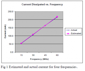
Our measurements and simulation results showed that within the domain of circuits with homogenous routing complexity and fanout, our model is able to predict power dissipation with a reasonably high degree of accuracy, while varying size, frequency and toggle rate (Fig1). Kslices was determined to be .0043.
However, this model does not seem to lend itself to estimating power in circuits where the nets vary widely in terms of fanout and routing complexity, since it uses an average toggle rate and the nets may have dramatically different loads. To solve this problem, we decided to use a model where the size of the design is measured in terms of total wires. The power is essentially calculated separately for each wire and totaled using the same procedure used previously to calculate the toggle rate. Since the wires specified in the design’s netlist do not correspond directly to the actual wires present in the placed and routed design which is loaded into the FPGA, the design is run through the vendor’s synthesis tools and then back annotated to show which nets should be counted during simulation. Our results show that this model works as well as the former in accurately predicting power dissipation.
We are currently working on verifying this model in circuits with varying fanout and developing a heuristic for estimating routing complexity. Another goal is integrating this system with JHDL’s graphical circuit browser, so designer can get a visual representation of the circuits power consumption.
References
- Weiss, Karlheinz: Power Estimation Approach for SRAM-based FPGAs. ACM/SIGDA International Symposium on Field Programmable Gate Arrays (FPGA), Monterey, CA, 2000.
