Nathan Whitehead and Shiuhhua Wood Chiang, Electrical & Computer Engineering
Project Overview
The goal of this research was to demonstrate that the complementary and 4-stage amplifiers can achieve superior gain or speed over the 2-stage charge-steering amplifier in [1], and the conventional differential amplifier introduced in the ORCA grant proposal. The completion of this project has involved schematic design, layout, test bench setup, amplifier measurements, and characterization.
Layout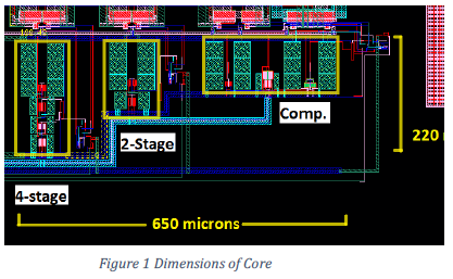
The three amplifiers take up a 650μm X 220μm area as shown in Figure 1. This includes the clock generation circuitry for the buffers. Each amplifier includes dummy transistors to shield the transistors from any manufacturing inconsistencies. This helps to maintain the symmetry of the amplifiers and suppresses offset. Ideally, the offset is zero, which is when the right branch is identical to the left. MOM (metal-oxide-metal) type capacitors are used as load capacitors for each of the amplifiers.
Gain Characteristics
The 2-stage amplifier was designed to have a gain of 16. For a 1 mV differential input the differential output is 16 mV. This is the ideal gain from simulation. Figure 2 shows the gain curve that is based on collected data from the fabricated chip 𝛥𝑉𝑂𝑈𝑇 is the differential output and 𝛥𝑉𝐼𝑁 is the differential 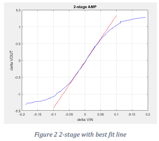 output. The gain curve begins to saturate at about 50 mV or – 50 mV for 𝛥𝑉𝐼𝑁. The slope of a best fit line determines the gain of the amplifier. In this case the slope,
 ![]() [insert picture that way →]. Percent error of the measured gain compared to the theoretical gain is 13.9 %. Note that when 𝛥𝑉𝑂𝑈𝑇 = 0, 𝛥𝑉𝐼𝑁 does not equal zero. This is due to the offset as discussed earlier. 𝛥𝑉𝐼𝑁 = 3.5 𝑚𝑉 when 𝛥𝑉𝑂𝑈𝑇 = 0, this is the offset.
[insert picture that way →]. Percent error of the measured gain compared to the theoretical gain is 13.9 %. Note that when 𝛥𝑉𝑂𝑈𝑇 = 0, 𝛥𝑉𝐼𝑁 does not equal zero. This is due to the offset as discussed earlier. 𝛥𝑉𝐼𝑁 = 3.5 𝑚𝑉 when 𝛥𝑉𝑂𝑈𝑇 = 0, this is the offset.
The complementary amplifier has both a theoretical gain (gain from schematic simulations) of 5.7 and 6.7. The two gain measurements come from the amplifier having two outputs, one is the output from the positive edge amplification phase and the second from the negative edge.
Figure 3 shows the actual measured differential output voltages. Both differential outputs have similar gain but different offset. The two differential outputs share about the same slope and thus have the same ![]() gain, which is [insert picture ←].
gain, which is [insert picture ←].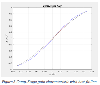
To measure the gain of these amplifiers an IC buffer was used in order to produce a differential input. However, there exists noise at the input which causes the output to flicker. This makes it difficult to get an accurate measurement at the output. Although noise is present, the oscilloscope averages the output voltage to help compensate for the noise. The values plotted in Figures 2-4 are the average voltage output. Due to noise being present at the input, the gain of the 4-stage amp cannot be easily characterized. It has a much higher gain and the input noise is of similar magnitude to the full input range of the amplifier. This does show, however, that this 4-stage design can achieve higher gain with only slightly more power draw than the 2- stage amplifier. In addition, the complementary stage is twice as fast as the 2-stage amplifier due to double throughput.
Clock Generation
These amplifiers operate on a clock which is CK in Figure 4. All three amplifiers use the same clock generation circuit. CKD is delayed by td1=250ps. In the 4-stage amplifier, CKD provides time for the first two stages to have a valid output before it acts as an input to the third stage. CKN, CKNB, CKND, and CKNDB are clock signals used for the sample switch of the buffer stage in Figure 5. At time t0, CKN  is low and CKNB is high and VCM is the input to the source follower (buffer stage). The source follower then switches its input to the output of the amplifier at t1. The delay, td2, helps the switch, implemented as two transmission gates, to not pass VCM and the amplifier output at the same time. The amplified output is shown on the output of the buffer stages between t1+td2 and t2. This repeats for every CK cycle. Figure 4 shows the clock signals needed for the 2-stage and 4-stage amplifiers and both use two buffers. The complementary amp. uses four buffers. It has two differential outputs where each differential output has two single ended outputs. In other
 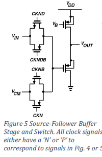 words, each buffer passes only one single ended output. The signals in Figure 4 still apply for the complementary amp. But require a set of four more clock signals for the additional two buffers. Figure 5 shows these signals in relation to the orignal CK. Note that CK in Figure 4 is the same as CK in Figure 6. CKP, CKPB, CKPD, and CKPDB are all the same waveforme as their counter part signals in Figure 4 except they are shifted by TCK/2. This is to pass the amplified signals to two other buffers from
 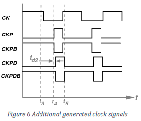 the amplified signals due to the falling CK edge.
Scholarly Sources
[1] Chiang, S.-H.W.; Hyuk Sun; Razavi, B., “A 10-Bit 800-MHz 19-mW CMOS ADC,” in Solid-State Circuits, IEEE Journal of , vol.49, no.4, pp.935-949, April 2014
