Cody Petrie and Steven Turley, Department of Physics and Astronomy
Introduction:
Reflection of extreme ultraviolet (EUV) light is made difficult by a number of factors. First, most materials have a large, imaginary part of the index of refraction for EUV light, causing absorption. As a result, our experiment is done under vacuum. Second, since the wavelength of EUV light (1-100 nm) is smaller than visible light, it is scattered more strongly than visible light. To overcome this obstacle we need to make our reflecting surfaces smoother. To be able to do this we need a good probe for surface roughness on the scale of EUV wavelengths. Currently the best method for measuring thin film roughness is atomic force microscopy (AFM). The AFM consists of a small tip on the end of a cantilever which is moved across a rough surface. As the tip moves up and down with the surface the movements are recorded by reflecting a laser from the end of the cantilever. However, the AFM does not have the resolution1 necessary to measure roughness on the scale of EUV wavelengths. As a result, we have used EUV reflection to probe surface roughness by reflecting EUV light from a surface and comparing it with calculations from model rough surfaces.
Methodology:
We have taken reflection measurements at the advanced light source (ALS) in Berkley California. The ALS uses synchrotron radiation to perform experiments. Our experiment was done on beamline 6.3.2 which is dedicated to EUV reflectometry experiments. We reflected EUV light from a thin film and measured how much light is reflected as a function of angle using a channeltron detector. We compared these measurements to two different reflection calculations from random model surfaces. We varied the roughness of the model surfaces until the calculated reflection matched the measured reflection. Once the reflection profiles agreed we concluded that the real surface had the same roughness as the model surface. The calculations that we did were geometrical optics (GO) and physical optics (PO). The GO calculation is simple and quick, but at the expense of accuracy. We used GO to qualitatively understand the large wavelength features of our thin films. The PO calculation is more accurate, but more computationally expensive than the GO calculation. We used PO to fit the short wavelength roughness features of our thin films. These are the features that the AFM does not have the resolution to probe. However, by definition our method has sufficient resolution since we are using the same light to measure roughness that we will be using to make mirrors for later.
The model that we used for our model surfaces had two parameters. The rms roughness height and the width of the spatial frequency distribution, assuming a Gaussian distribution.
1 K. L. Westra and D. J. Thomson, “Effect of tip shape on surface roughness measurements from atomic force microscopy images of thin films,” J. Vac. Sci. Technol. B 13, 334 (1995).
Results:
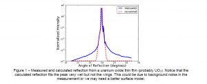
Figure 1 shows a characteristic reflection measurement as well as the calculated reflection that fit the measured reflection.

These measurements were done on two uranium oxide thin films of different roughness. One had a thickness of 44.4±1.3 nm and the other 412.9±7.0 nm. Figure 1 shows the results of one measurement on the 412 nm film. The rms roughness height that we determined for the 412 nm sample was 0.78±0.15 nm and the width of the spatial frequency distribution was 8.3e-5±2.7e-5 nm-1.
Discussion:
We were not able to find a fit for the 44 nm sample. This may be due to large scale (order of hundreds of nm) bumps on the surface. However we were able to get a qualitative understanding of these bumps using GO. Using PO were able to fit the peak of the reflection from the 412 nm sample. We were not able to fit the wings of the reflection however. This may be due to background noise that was not accounted for in our analysis. This discrepancy could also be due to a weakness in our surface model. As a result we will be improving our model, and trying new surface models in the future. It would also be due to assumptions made in the PO calculation. To overcome these assumptions we will be using a calculation that is derived directly from Maxwell’s equations2.
Conclusion: We have developed a method for measuring the roughness of thin films that will aid the process of making smooth surfaces for EUV optics. With this method we have measured the rms roughness of our 412 nm film to be 0.78±0.15 nm and the width spatial frequency distribution width to be 8.3e-5±2.7e-5 nm-1. Future work includes improving the surface model, using a more exact calculation, and repeating the work for a variety of thin films.
1 K. L. Westra and D. J. Thomson, “Effect of tip shape on surface roughness measurements from atomic force microscopy images of thin films,” J. Vac. Sci. Technol. B 13, 334 (1995).
2 J. E. J. Johnson, Master’s thesis, Brigham Young University, 2006.
