Hannah Quist and Dr. Aaron Hawkins, Electrical and Computer Engineering
Main Text
Ion trapping is a method of determining the elemental composition of a charged sample, allowing the substance to be properly identified. It uses metal rings or lines with an applied voltage and radio frequency to initially trap the ions in a central region and begin to eject successively larger ions as the radio frequency is increased.
Miniature ion traps are more portable than their larger counterparts. BYU has been a leader in the design of miniature ion traps that are made using ceramic plates and microfabrication. There is significant interest in using our capabilities to produce a new design – a linear ion trap that can contain more ions than previous circular designs. After receiving funding from the ORCA grant, I was able to begin work on fabricating miniature linear ion traps.
First, I needed to determine a design that would be efficient in trapping and releasing the ions in the trapping region. An ion simulator program was used to test various line placements for their response to changing voltages and radio frequencies. The electric field in between the ion trap plates was compared to a standard trapping field to ensure that the charged ions would follow the desired pathway of ejection. An important part of the design is to be able to manipulate the higher polar components affecting the electric field, so it was decided to have the lines of the trap lay along the axes of these polar components. This information was also used to determine how long of a slit was necessary for efficiently ejecting ions from the system.
A printed circuit board (PCB) was created for each desired voltage configuration. The PCB contains a network of voltage dividers (using capacitors) to create a voltage drop of a desired value between each ring or line. Gold spring-loaded pins are then used to transfer the PCB’s voltage to the via thru holes (which are filled with gold) on the ceramic plates.
Once the design parameters were set, I used AutoCAD to create a pattern for the desired plates. I drew and labeled dimensions for the body of the ceramic plate, the slit used for ejecting ions, and the vias. I then sent this design to a company that created the ceramic plates.
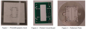
After finalizing the plate design, I designed the photolithography mask for patterning the lines onto the plates. This required designing two different lithography masks—one for the side with lines and one for the side with pads for applying voltages through the vias to the lines. This involved using a Cadence program to draw how I wanted each side of the plate to appear after patterning. We then sent this pattern to another company who produces photolithography masks (Figure 1).
To design the necessary PCBs for the project, I used a program called Eagle so that I could place holes for the spring-loaded pins, patterns for soldering capacitors to get the desired voltage drops, and traces connecting these items in the proper configuration. This file was then sent to a company that produces PCBs (Figure 2).
When I received the plates, photolithography mask and PCBs, I began the fabrication process. First, I focused on developing correctly patterned plates. This was done in a series of processes each completed in BYU’s clean-room facility. I start out by cleaning all particles off of the plates so that the metal traces were able to effectively stick to the surface. I then evaporate the metal, either gold or aluminum, onto the plates so that the entire surface was coated. After evaporating on both sides, I coated the surface with a layer of spin-on resist and used our photolithography machines to expose the pattern on one side. The extra photo resist was removed and the plate was then placed in an etchant that removes the gold or aluminum. The photo resist pattern was then removed. After both sides of the plates underwent this process, a layer of germanium was evaporated onto the line side of the plates to prevent charge build-up on the ceramic.
This process required a great deal of troubleshooting because of the sometimes unavoidable faults in fabrication. Sometimes during the process, part of the patterned gold can be scratched, severing a necessary connection, or one of the vias does not have a good connection with the pattern around it and an epoxy is necessary to make the connection more complete. After several iterations of this process and overcoming several setbacks, I was able to produce plates with complete connections that could be used in testing (Figure 3).
After fabricating working plates, I focused on creating PCBs with desired electric fields. This involved choosing voltages that would produce the electric field and calculating what capacitance values were necessary to develop the desired voltage stratification. After determining these capacitance values, I used a capacitance-voltage meter to pick out capacitors within a certain tolerance range. I then soldered these capacitors to the PCB and reconfigured the connections between capacitors as needed.
Currently, the system is assembled with all the necessary fabricated parts. A graduate student colleague is currently developing a radio-frequency scanning series that will produce mass dependant spectra for arbitrary test samples. My research results have already been presented at a conference1 and I expect to publish further results in the future.

