
Oliver Johnson and Dr. David Fullwood, Mechanical Engineering
Main Text
The development of a large-strain sensor technology will open doors for improved engineering design and scientific research in many fields. Such a technology would allow for advances in biomechanical engineering, e.g., prosthetic limb and artificial organ design. Additionally this kind of sensor technology could be used for tactile robotics and even structural health monitoring, such as in wind turbines or architectural structures. Our research group has developed a unique Silicone/Nickel Nanostrand/Nickel Coated Carbon Fiber (Si/NiNs/NCCF) nanocomposite that can measure strains of up to 50% elongation. The purpose of this project was to investigate how the nano-scale structure of this material may influence its piezoresistivity. Since charge transport in conductive polymer composites depends greatly upon the distance between conductive particles, our goal was to experimentally measure the inter-particle distance distribution.
We interrogated a 9μm x 11μm x 17μm (1614 μm3) volume of Si/NiNs/NCCF using a dual-beam focused ion beam/scanning electron microscope (FIB/SEM). This tool allowed us to collect serial micrographs throughout the volume. In order to probe the nano-structure of the material, the images that we collected needed to be used to reconstruct the 3D volume. Originally we had planned to use commercially available software for the reconstruction; however, the amount of manual user interaction required was prohibitively large. As a result I wrote code in Matlab® that automated the reconstruction process substantially. This code performed the following tasks: data import; image registration; volume cropping; image segmentation; and connectivity analysis. Image segmentation is the process of taking a grayscale image and identifying pertinent objects. In our case we needed to identify in each image what pixels corresponded to Nickel and what pixels corresponded to Silicone. Traditional image segmentation methods gave very poor results. Therefore, I implemented an advanced segmentation algorithm known as the EM/MPM algorithm [1]. This technique assigns pixels to a given class (Ni or Silicone) based on their value and their context in the image (i.e. the grayscale value of their neighbors). This resulted in a much improved segmentation. Another obstacle that had to be overcome was that of correctly identifying which objects in a given image were to be connected to which objects in neighboring images. Originally we simply extruded each Nickel cross-section into the subsequent image and wherever Nickel overlapped Nickel we assumed that those cross-sections were connected. This approach resulted in over-connectedness. In order to improve the accuracy of our connectivity, I developed a new connectivity algorithm, based on principal component analysis (PCA), that takes into account the shape and context of each cross-section in determining what cross-sections in the neighboring images to connect to. The basic idea is to assume that NiNs branches are essentially cylindrical so that oblique cross-sections of these branches are elliptical. Using PCA one can determine the major and minor radii of each cross-section and, by extension, the axis of the assumed cylinder. We tested this method on a synthetic nanostructure and were encouraged by the accuracy of the results.
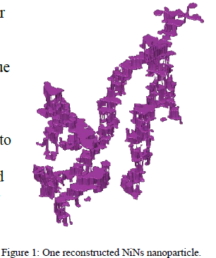
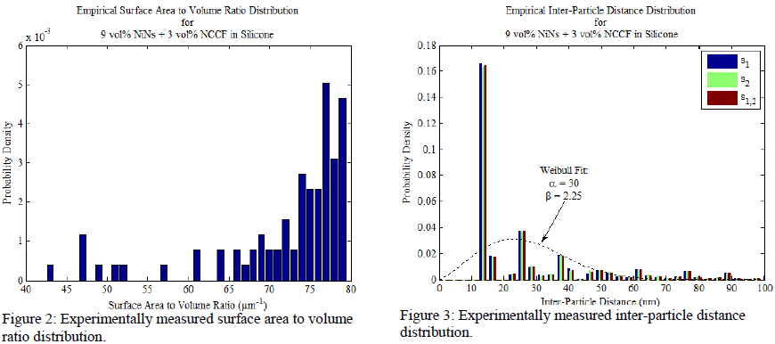
After reconstructing the volume of material using the code that I developed (see Fig. 1), I wrote further code to measure various nanostructural properties: the distribution of nanoparticle surface areas; the distribution of nanoparticle volumes; the distribution of nanoparticle surface area to volume ratios; and the distribution of inter-particle distances. The results indicated that NiNs are highly bifurcated with surface area to volume ratios tending towards ~80 (Fig. 2). The inter-particle distance distribution corroborated our hypothesis that the distances follow a wiebull like distribution (Fig. 3). Since the pixel resolution was ~12.5 nm the first bar in Fig. 3 is, in reality, spread over the domain from 0-12.5nm. With higher resolution the empirical distribution can, therefore, be expected to follow the theoretical curve more closely.
A colleague and I presented preliminary results from this project at the 42nd International SAMPE Technical Conference, which were subsequently published as a part of the conference’s collected proceedings [2-3].
Acknowledgments
I would like to thank Michael Standing for performing the FIB/SEM sectioning, George Hansen for providing the Nickel nanostrands that we used, and Matt Converse for his collaboration.
References
- Comer, M., Delp, E., “The EM/MPM algorithm for segmentation of textured images: analysis and further experimental results.” IEEE transactions on image processing. 9.10 (2000): 1731-44.
- Johnson, O., Fullwood, D. “A Percolation/Quantum Tunneling Model for the Unique Behavior of Multifunctional Silicone/Nickel Nanostrand Nanocomposites.” 42nd International SAMPE Technical Conference, Society for the Advancement of Material and Process Engineering (SAMPE), Salt Lake City, UT, October 11-14, 2010.
- Converse, M., Johnson, O., Fullwood, D. “Quantification of Nickel Nanostrand Distributions within a Silicone Matrix using a FIB/SEM System.” 42nd International SAMPE Technical Conference, Society for the Advancement of Material and Process Engineering (SAMPE), Salt Lake City, UT, October 11-14, 2010.