Meagan Bracken and Dr. Aaron Hawkins, Department of Electrical and Computer Engineering
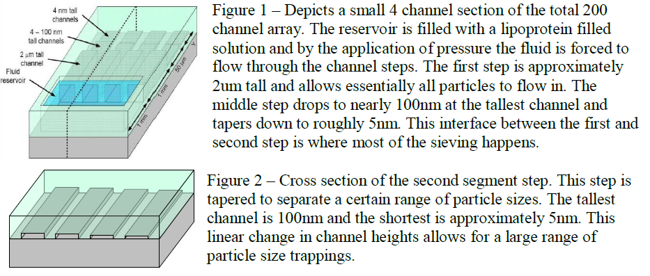
The purpose of this project was to assist in the manufacturing of nanosieves. The device is designed to separates nano-size particles from the fluid substance in which they are contained. An example of this, and one of the main targets of this project, is the separation of HDL and LDL cholesterol particles from a sample of blood. This goal of separating cholesterol has many benefits to the medical world. By creating a method to characterize HDL cholesterol sizes and concentrations we can monitor a person’s risk for heart disease. Because cholesterol particles have this important attribute of size characterization, it would be desirable to create a system of nanotubes, varying in height that could capture a particular size of nanoparticles.
The sieving system works by taking a sample of biological particles and labeling them with a fluorescent marker. By running the sample through an array of nanotubes which slowly decrease in height, we can separate the particles according to their relative sizes – allowing for size characterization. The subject of my research project focuses directly on this creation of tapered nanotubes. These tapered channels can be easily and cheaply built by using a material called photoresist. When exposed to UV light the emitted radiation causes a change to occur in the molecular structure of the photoresist. This change allows exposed areas to be removed when put in a developer (300MIF). This property allows us to pattern some rather intricate structures onto the surface of our silicon wafer. My research uses this same process to build a tapered array of 200 channels.
Photoresist has a non linear exposure to development relationship which causes a great difficult when creating these linear tapered channels. Instead of developing away linearly with varied exposure, the photoresist tends to peel off in steps. There were a number of methods we used to try and create these tapered photoresist wedges but the best results came from using a stationary PMMA exposure method. We first started by creating large wedges out of different colored plastics using a laser cutter. The cuts were rough and had to be sanded down using a very fine grain to remove as many flaws as possible. The results were quite good from these initial wedges; however, the structures were much larger than we needed for our chips.
![]()
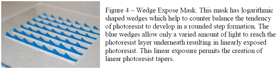
The next step was to miniaturize our taper structures. This sounds simple enough, however we found that photoresist particularly does not like to taper over a short area. The tendency however is to create rounded steps in the taper so that it is no longer linear across the entire profile. To counter this stepping problem, I created a mathematical formula from our previous results and our desired result to create a plastic wedge will would counter act with the tendency of the photoresist. It turned out that the required plastic wedges were logarithmic in shape.
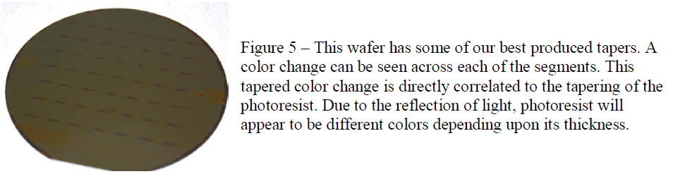
The second large problem we faced dealt with the development time of our photoresist. Because we are dealing with structures approximately 150 nm tall and shorter, we have to heavily dilute our photoresist. Our original diluting substance is NMP and allows us to get very thin layers of photoresist. However, at very thin thicknesses photoresist is developed away quickly and is not as easily controllable. After research on the matter we found that we could instead dilute the photoresist with PGMEA which is a more natural substance to the resist. This change allowed us to more easily control the development of our wafer. Rather than developing away in 20 seconds, we now have a 90 second development time. This slower development is not only much easier to monitor, but it is much less abrasive. Because the photoresist is being developed down to such small layers, we faced a problem when our thinnest taper height becomes almost as small as the particles within the photoresist. These small features caused the thinnest layer of photoresist to want to pull of the surface of the wafer very easily. However, with the new diluting substance this is now much easier to avoid. The tapers are not entirely finished and there is still room for improvement – consistency being a big one of them. However, the tapers have made significant progress and are very pleased with what we have found and with their current implementation.