Christian A. Fox and Dr. Richard H. Selfridge, Electrical and Computer Engineering
During the past decade, much research has been invested in the optics field to develop high-speed optical modulators. In particular, efforts have been directed toward combining the fast electrical responses of nonlinear optical polymers with the light guiding characteristics of fiber optics.1 At Brigham Young University, recent efforts have been made to develop a low-loss polarimetric modulator integrated onto a standard silicon wafer. This paper will discuss the fabrication process, present experimental results, and suggest further improvements for the fiber optic modulator.
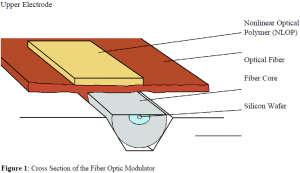
A major portion of the modulator’s fabrication takes place in BYU’s Integrated Microelectronics Laboratory. First, a D-shaped optical fiber is entrenched in a groove etched into a standard silicon wafer. The D-fiber is used because it has a planar side which lies close to the core of the fiber, or the region where most of the light signal propagates. The silicon wafer provides support to the fiber, aids in processing steps, and serves as an electrical ground plane. Once the fiber is secured in the groove with the flat side parallel to the wafer surface, its planar side is etched down with a hydrofluoric acid solution to within a half-micron of the fiber core.
Once the etch is complete, a thin nonlinear optical polymer (NLOP) layer is placed on top of the fiber (see Figure 1). The NLOP consists of large host molecules (PMMA) and long-chain guest chromophores (Disperse Red 1 or DR1). In order for the modulator to function properly, the NLOP layer must be poled, which includes the mass aligning of the long-chain chromophores. This poling process is carried out at an elevated temperature near the glass transition state of the polymer in order to maximize chromophore rotation under an intense electric field.2 Cooling the NLOP under this electric field immobilizes the molecules and establishes an electro-optic coating in close proximity to the fiber core.
Following the poling process, an upper electrode is deposited on top of the poled portion of the NLOP layer. As a voltage is applied across the electrode and the grounded silicon wafer, the refractive index of the NLOP changes. This change results in a variation of the polarization characteristics of the propagating light signal. Under a polarization filtering configuration, where the input signal is linearly polarized at 45 degrees to the principal core axis, output light modulation corresponding to the frequency and magnitude of the applied voltage may be detected through an analyzer.
It is anticipated that this polarimetric modulator is capable of reaching frequencies higher than 100 GHz, five to ten times faster than the standard high-speed modulators currently being used. This type of success, however, has not yet been achieved. Frequencies up to 400 kHz have been observed with our fiber optic modulator, but it has been concluded that other factors have produced the modulation. These causes include piezoelectric responses of the NLOP layer to the applied voltages and a corresponding vibration of the optical fiber itself. Thus, physical straining of the fiber has been the cause of the limited modulation instead of an electro-optic interaction. Because the strain-induced modulation is cut off at high frequencies, it should not present a problem for the desired high-speed switching.
The current focus to improve the modulator is centered on the NLOP layer. This thin film, which is presently made up of a PMMA/DR1 mixture, has an index of refraction higher than that of the fiber core (1.52 and 1.48 respectively). However, in order to have the propagating light signal remain in the optical fiber, the material surrounding the core should have a refractive index less than 1.48. New nonlinear optical polymers are being explored to replace the current NLOP. Also, work is being done to verify that the NLOP is being poled and that the guest chromophores in that layer are aligning properly. This verification process is being carried out through second harmonic generation experiments.
The fiber optic modulator integrated on a silicon wafer has the potential to become an important step in the optics field. Its low-loss properties and cost-effective design make it a favorable addition to situations where high bandwidth communications are needed.3
References
- Hamilton, S.A. et alia. “High Bandwidth Traveling Wave Polymeric In-line Fiber Modulator.” CLEO ‘97 Technical Digest. 1997: 293.
- Mortazavi, M.A. et alia. “Second-harmonic Generation and Absorption Studies of Polymerdye Films Oriented by Corona-onset Poling at Elevated Temperatures.” Journal of the Optical Society of America B. April 1989: 733-741.
- Special thanks to G.C. Harston and M.V. Pack of the Department of Electrical and Computer Engineering and R.E. Wilson of the TransEra Corporation for their support in this project.

