James Owen Ostler and Dr. Bret C. Hess, Physics and Astronomy
With diameters of only about 4-5 nanometers, semiconductor nanocrystals exhibit different properties than bulk semiconductors. Because of this there has been a focus in research to discover and exploit these new properties. The CdSe nanocrystal is smaller than the normal wave function of an electron in bulk semiconductors and this produces different properties in the nanocrystals than what current knowledge about semiconductors would dictate. Our experience with the different physical properties of these quantum-confined semiconductors is limited, however the possible uses for these nanocrystals are numerous. This necessitates that we research and familiarize ourselves with the properties of these nanocrystals in order use them in these applications and discover new possible applications. Current research with CdSe nanocrystal films by current injection has shown potential in the areas of photoluminescence, and electron spin resonance in order to give clues into the charge distribution of the nanocrystals. New methods of research are also needed in order to deal with these new nanoscale semiconductors. This has been the focus of my research.
Diodes made from these CdSe nanocrystals have been shown to exhibit decreasing current density versus time across the diode. It has been proposed that this drop of excess charge is due to the filling of deep traps of the sample. This would correlate with the observations of time-dependent light output in LEDs, which has also been attributed to charge storage effects.2
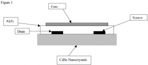
My original plan was to construct a diodes by preparing the nanocrystal film by spin coating the nanocrystals, in a toluene solution, onto indium-tin oxide (ITO) coated glass substrates, then depositing on top of the nanocrystals an aluminum coating by thermal evaporation. However, this method proved to be very tedious and difficult mainly because of the problems that were presented in trying to cut the ITO into small enough sizes to appropriately test them. Because of this other methods of testing were considered. This actually turned out to be a blessing in disguise for as we searched through journals for other ideas we came across a method that used a transistor in place of a diode in a similar fashion testing the properties of C60.3 (Refer to figure 1)
Using a transistor not only allowed us to study the same properties as would be possible with a diode, it also opened up the door to new more effective tests.
We then focused on designing a transistor that would accomplish our goals in this project. This proved to be the majority of the project. We decided to use thin transparent wafers and then use a combination of evaporation and etching techniques to make the transistors. On a four-inch wafer we are able to produce approximately 120 transistors. We used a computer program to help create a film print with the three design steps that are necessary to produce this transistor.
The method used to etch was another concern. A method was needed that would remove the unwanted material without damaging the necessary structure of the transistor. We were limited in out options by the equipment that the clean room possessed. This required us to develop a new method to etch the transistors. With the help of the clean room operators we successfully developed a method to accomplish this.
The research is continuing on from this point. The design and masks for creating the transistors is completed and very soon testing on the transistors will be started.
Bibliography
- M. Nirmal, B.O. Dabbousi, M.G. Bawendi, J.J. Macklin, J.K. Trautman, T.D. Harris, and L.E. Brus: Fluorescence intermittency in single cadmium selenide nanocrystals. Nature; 31 Oct 1996; Vol. 383 p. 802-804
- D.S. Ginger and N.C. Greenham: Electrical injection and transport in films of semiconductor nanocrystals. Journal of Applied Physics; 1 Feb 2000; Vol 87 no3 p.1361-1368
- J. H. Schon, Ch. Kloc, R. C. Haddon, B. Batlogg: A Superconducting Field-Effect Switch. Science; 28 April 2000; Vol 288 p. 656-658

