Dale S. Kitchen and Dr. Robert C. Davis, Physics and Astronomy
This report describes the growth of carbon nanotubes on sharp silicon cantilevers through chemical vapor deposition (CVD) and the implementation of thin film and acid etch techniques to shorten the grown nanotubes. Silicon and silicon-nitride probes serve as the principle imaging tools for Atomic Force Microscopy (AFM). Carbon nanotubes may serve to enhance the imaging stability and resolution of AFM through their unique properties. Herein, I describe procedures, explain the presented results, and outline future work on this project.
Many important surfaces, such as cell membranes and solid-state devices, do not conduct electrons sufficiently or are quickly damaged by the probing electrons of electron microscopes. To circumvent this problem, AFM approaches surface measurements from a mechanical interaction between a probe and the surface. A sharp probe at the end of a long cantilever arm moves across a surface much like a record player needle, electrically recording the mountains and valleys of a surface. While the sharp silicon probes have enabled resolution of surface materials previously not resolved, the fabrication process of conventional probes self-limits the achievable resolution in the radius of curvature and the aspect ratio.
Carbon nanotubes have the potential to improve imaging resolution by more than a factor of ten, as well as to improve the reliability and robustness of AFM imaging tips. Nanotubes consist of a single enfolded sheet or multiple enfolded sheets of graphene that give them a cylindrical shape. They have been classified as single-walled nanotubes (SWNT) and multiple-walled nanotubes (MWNT). These narrow tubes often have lengths on the micron scale—many magnitudes longer than their cross-sectional radii. We are interested in the use of SWNTs because of their small radius of less than one nanometer and excellent aspect ratio. Furthermore, SWNTs exhibit a high degree of flexibility without degeneration making them vigorous against breaking.
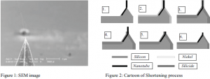
We have used established techniques to grow SWNTs in a CVD environment after dipping the silicon cantilevers in a suspension of nanosized metallic particles that act as a catalyst to start nanotube growth. The CVD process grows nanotubes over the surface of the silicon tips. When a nanotube grows from a catalyst site towards the apex or end of the tip, it extends off the surface rather than growing around the sharp bend of the tip end (Fig. 1). These nanotube tips extend several hundred nanometers past the silicon tip end, causing them to buckle easily. Current processes to shorten the nanotube tips are slow and tedious. The following describes the development of a uniform, multi-probe, shortening technique. This process has the potential to be faster, to create nanotube tips of uniform and precise lengths, and to be implemented on an entire silicon wafer containing hundreds of silicon probes.
Our shortening technique makes use of thin film and acid-etch techniques. Figure 2 displays a cartoon that shows the basic steps of this process. A thin film of nickel is deposited over the silicon and nanotube tip (Fig. 2.2). Next, a thermal silicidation process enables the nickel and silicon interface to form an alloy, nickel silicide (Fig. 2.3). A piranha etch then removes the nickel metal that did not convert to silicide, in particular the nickel coating the nanotube tip (Fig. 2.4). An oxygen-plasma directional etch can then burn the exposed tube, leaving only the nanotube tip embedded in the silicide (Fig. 2.5). A final buffered hydrofluoric acid (BHF) dip allows the controlled removal of a portion of the nickel silicide layer to expose the desired length of the nanotube tip for imaging (Fig. 2.6). This should leave the nanotube embedded below the remaining nickel silicide layer with a desirable length of tube exposed at the tip end.
While the described shortening technique has not been fully realized on a nanotube tip, the following results of the shortening steps on wafer substrates show that implementation on the AFM probe is probable. First, nickel films of ten to fifty nanometers were evaporated on silicon wafer substrates with and without a BHF dip that removed the native silicon dioxide (SiO2). SEM images of the nickel films on the AFM probes were smooth on the silicon surface and appeared to cover the nanotubes. The nickel silicide layer formed successfully on silicon wafer substrates in a furnace of 500 to 600 °C during formation times of two to ten minutes. It was found that a nickel silicide layer formed on samples with and without removal of the native SiO2. The silicide with the SiO2 present did not etch under the piranha, but visibly partially etched with the BHF dip, just as the samples without SiO2. The piranha etch successfully removed the nickel film while visibly leaving the nickel silicide unchanged. In addition, samples showed that neither the BHF dip nor the piranha etch harmed the nanotubes. The nanotubes appear to remain evenly distributed after the deposition of the nickel film and after the formation of the nickel silicide. No results showed a lack of structural stability of the nanotubes in these processes.
The verification of several steps of this new shortening process indicates that nanotube tip growth and shortening could be applied at the industry level on entire wafers of silicon probes. Reliable nanotube growth through CVD has been achieved, as well as the ability to grow a nanotube tip on AFM silicon probes. Nickel films were successfully evaporated and nickel silicide was shown to form both with and without removal of the native SiO2 prior to nickel evaporation. Likewise, the piranha etch was shown to etch nickel metal entirely, while it did not etch the nickel silicide. The BHF dip etched controllable amounts of the nickel silicide layer. Upon further application of the shortening process to the AFM probes, the potential exists to provide more stable and uniformly shortened nanotube tips than those currently produced.

