Matthew Housley and Dr. Robert Davis, Physics and Astronomy
Atomic Force Microscopy (AFM) is currently one of the most important analytical techniques in nanoscale science and technology. Because it can image surface topography with a resolution better than 10 nm, AFM has allowed the visualization of many nanoscale structures which other microscopic techniques cannot see. Examples include individual DNA strands, extended polymer chains, monolayer steps in crystal surfaces, and carbon nanotube transistors.
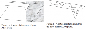
AFM works by essentially “feeling” a surface with a microscopic stylus or probe. The primary factor currently limiting achievable AFM resolution is probe tip geometry. Resolution is roughly equal to tip radius. At present, the sharpest commercial probes have tips with radii as small as 5 nm.1
Recently, interest has developed in making tips for AFM probes using carbon nanotubes. Carbon nanotubes are seamless cylinders of carbon that can have radii of less than .5 nm.2 Thus, they could potentially allow a tenfold improvement in AFM resolution.
Techniques have been developed to grow nanotubes on commercially available silicon AFM probes by chemical vapor deposition (CVD). Briefly, commercial probe are coated with alumina particles embedded with iron and molybdenum catalyst. The probes are then heated to 800°C in a tube furnace under a flow of hydrogen and argon. When the furnace has reached the target temperature, a small flow of ethylene is introduced. The ethylene decomposes on the catalyst embedded alumina particles to grow nanotubes all over the probes’ surfaces. Usually, one of the nanotubes on the surface of each probe will grow from its tip in a geometry useful for AFM imaging (Fig. 2).3 Yields as high as 90% have been reported with this process.
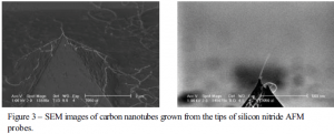
In my work, I initially applied this technique to silicon probes as had been previously reported. I then wished to extend the versatility of the process by extending it silicon nitride probes. This proved not to be as straightforward as I expected. Initially, the yield on silicon nitride probes was zero. However, I found that by coating probes with a thin layer of silicon (10 nm) before catalyst deposition, I was able to increase this yield to roughly 10%.4 Examples of successful nanotube tip growth are shown in figure 3.
Because the yield improved substantially with the addition of a silicon coating step, it is believed that the uncoated surfaces of the silicon nitride probes I used may have deactivated catalytic growth of nanotubes. However, the results remain inconclusive. There are also probably additional unknown issues that have kept the yield at 10%, far from the 90% yield seen on silicon probes. It is believed, however, that additional research could elucidate these issues and increase yield substantially.
For me, this project was a dramatic illustration of some of the difficulties inherent in research. While I assumed that going from silicon to silicon nitride probes would make little difference in my process, it proved to lower yield dramatically. Furthermore, the reasons for this drop in yield proved extremely difficult to elucidate through continued experimentation. Incremental progress was made in improving yield, but the reasons for this improvement remain unclear. But in spite of the difficulty I encountered in this project, I still found it encouraging in that progress was still made as I persevered.
References
- See for instance Digital Instruments’ web listing of contact mode probe specifications (http://www.di.com/products2/NewProbeGuide/ContactModeProbes.html) and look at silicon and oxide sharpened silicon nitride probes.
- N. Wang, Z. K. Tang, G. D. Li, and J. S. Chen, Nature (London) 408, 50 (2000).
- Jason H. Hafner, Chin Li Cheung, and Charles M. Lieber, J. Am. Chem. Soc. 121, 9750 (1999).
- For more technical details on this process and the variations used in my experiments, see my honors thesis: “Direct CVD growth of carbon nanotubes on silicon nitride AFM probes”, Brigham Young University, 2001.


