Jed Whittaker and Dr. Robert Davis, Physics and Astronomy
It has been previously shown1 that silicon tetraacetate vapor thermally decomposes to a silicon dioxide thin film and gas phase acid anhydride at 160-170°C. Here a method is developed to anchor carbon nanotubes to atomic force microscope (AFM) tips with such a silicon dioxide thin film. Anchoring nanotubes to probe tips allows their high-resolution properties to be exploited in fluids for imaging biological samples. No tips were used as substrates in this experiment however, only silicon wafer pieces about 1 cm square. The silicon tetraacetate vapor was produced by heating it to 100-110°C, just below the melting point. This prevented it from evaporating too fast and recrystallizing on the silicon wafer surface before decomposing to silicon dioxide. The wafer surface was heated to 160-170°C so that the decomposition and silicon dioxide deposition could occur.
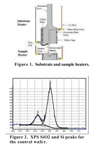
Two independently controlled heaters (figure 1) were made, one to control the temperature of the silicon wafer substrate, and the other to control the temperature of the silicon tetraacetate sample. Each had a manually controlled variac power supply, as well as a thermocouple for feedback. They were inserted into a flask, where a roughing pump created a vacuum of 70 mTorr. A shutter (not shown) was placed between them so that the recorded deposition time gave an accurate rate.
The control wafer piece was characterized first by x-ray photoelectron spectroscopy (XPS), which shows how atoms are bonded in a given sample. First, a survey of the sample revealed the presence of carbon, oxygen and silicon. Next, the characteristic peaks for silicon and silicon dioxide (silicon 2p shell) were investigated. The silicon peak normally appears at 98-101 eV, while the silicon dioxide peak normally appears at 100-103 eV. XPS of the control sample was in agreement with those values (figure 2). The silicon dioxide peak, on the left at 103.12 eV, had a relative area of 11,452.6. The silicon peak, on the right at 99.68 eV, had a relative area of 44,910.7. The ratio of the two shows that the silicon peak is 3.92 times bigger than the silicon dioxide peak. This is expected because the silicon dioxide film is thin compared to the silicon underneath, so there will be much more silicon than oxide. The deposition of a silicon dioxide thin film should increase the relative height of the silicon dioxide peak and decrease the relative height of the silicon peak, as the new film will be significantly thicker.
The original silicon dioxide thickness of sample 1 was measured by ellipsometry to be 27.332±0.069554 Å. Sample 1 was deposited on before the sample heater was built, so a hot plate was used instead. Some of the sample melted, due to the poor temperature control of the hot plate, leading to visible white chunks of recrystallized silicon tetraacetate on the wafer surface. The surface of the hot plate was measured with a thermocouple and was found to range from 105-125ºC; the melting point of silicon tetraacetate is 111-114ºC. Thermal grease was used as an adhesive on the back of the wafer because the wire clip had not yet been added, probably leading to contamination of the sample when it was cleaned off in acetone. The deposition happened for 30 minutes, although this is an estimate because the shutter had also not yet been added. Unfortunately no ellipsometry data was taken after the run.
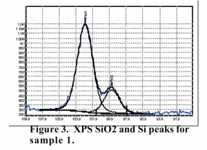
The XPS data for the deposited silicon dioxide (figure 3) show a clear distinction between the silicon dioxide peak and the silicon peak, which are at 102.86 eV and 99.62 eV, respectively. The ratio of their areas shows that the silicon dioxide peak is 3.63 times bigger than the silicon peak. This indicates that the silicon dioxide layer has thickened significantly as a result of the thermal deposition.
After adding the sample heater, the shutter, the wire clip and removing the remaining thermal grease from the heater, sample 2 was run. It had an initial silicon dioxide film of 17.772±0.070564 Å, measured by ellipsometry. The wafer substrate was held at a temperature of 163ºC by the variac at 8.0 Vac. The sample was held at a temperature of 100ºC by the second variac at 2.0 Vac. The lower temperature was intended to discourage the silicon tetraacetate from melting to the vapor phase. The system was in a vacuum at 70 mTorr, and the shutter was open for 20 minutes. The final silicon dioxide film thickness was measured by ellipsometry to be 139.61±0.25285 Å. Thus the deposition added 121.8Å of silicon dioxide in 20 minutes. Converting that gives a deposition rate of 0.1Å/sec, which agrees with the thermal deposition rate of a previous group’s work2.
More trials need to be done in order to produce a more accurate deposition rate, as well as to discover if the silicon dioxide will coat the nanotubes. One method for determining how the film interacts with carbon nanotubes will be growing the tubes over lithographically produced trenches, taking AFM images of them, depositing silicon dioxide and comparing the diameter of the same tubes after by AFM. It will be important to mark the spot where the original images were taken, as well as measure the diameter of the original tubes. This will allow characterization of the selectivity of deposited silicon dioxide for carbon nanotubes, and determine the usefulness of the process for producing nanotube-tipped AFM probes.
___________________________________
1 T. Maruyama and K. Aburai: Jpn. J. Appl. Phys. 27 (1988) L2268
2 T. Maruyama and J. Shionoya: Jpn. J. Appl. Phys. 28 (1989) L2253


