C. Alva Barney and Dr. Doran K. Wilde, Electrical and Computer Engineering
In conjunction with the ORCA research grant I was able to design, layout and simulate an integrated Synchronous Data Link Control (SDLC) communication chip. SDLC communication chips are commonly used to transfer data between computers in serial bit-wise transmission. Extensions of the SDLC are used in high speed data links and satellite communication. In addition, this project was accompanied with full web documentation such that the VLSI Design Class (ECEn 451) can leverage my research and design as a class project.
The completed design was submitted for silicon fabrication on a 1.2 micron process. The actual integrated circuit will be received in September 1998 and subsequently tested to compare the actual hardware with simulation results. The chip included over 4000 transistors with core dimensions of 2000 x 2000 microns. The total die size, including the padframe, is about 2300 x 2300 microns. This works out to be 2.3mm x 2.3mm or .053 square cm. The small die size would make this chip viable for high volume production.
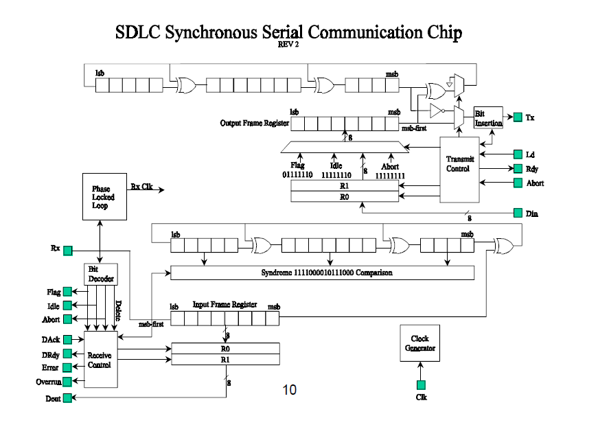
The SDLC communication chip is a state-of -the-art integrated circuit and adheres to industry standards. The finished design was simulated to verify proper functionality and performance. It included the standard SDLC transmitter and receiver with variable length data segments, bit insertion to allow all possible data sequences, and full error checking. The receiver included a custom phaselocked loop (PLL). As seen in the block diagram on the previous page, both the transmitter and receiver feature 2-level data registers. In addition, 8 state machines were used to control the SDLC communication chip. During the design project a PLL was added to recover phase and frequency from the incoming data and produce the receiver clock. This gives the receiver the freedom to receive from any SDLC transmitter which run in a certain frequency window. The PLL loop was fine tuned to allow data transmission rates from 10- 45Mhz with the center frequency set at 25Mhz.
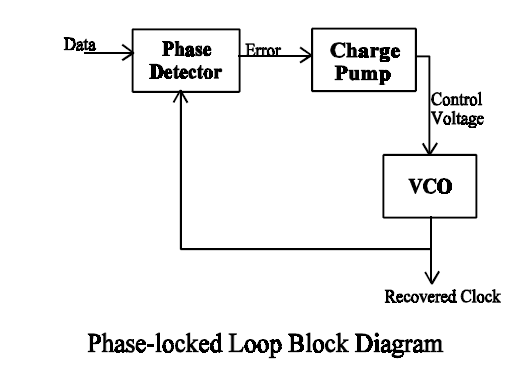
The PLL, as shown above, contains three basic building blocks. The phase detector compares the generated clock with the incoming data. It will then send a signal to the charge pump telling it to pump up or pump down the Voltage controlled oscillator (VCO) control voltage. The output clock is a function of the DC level of the control voltage. The PLL, allows the receiver to lock onto and accurately receive a transmission with out stringent phase and frequency requirements.
The overall research was successful and several new circuit ideas were implemented. I have gained valuable experience in both digital and analog design. In addition, the project will be leveraged as a class project by future students in VLSI design. For further information, see http://www.et.byu.edu/~barneyc/orca.html