Benjamin Frandsen and Dr. Branton Campbell, Physics and Astronomy
A wide variety of electronic devices, including microphones, acoustic transducers and high-powered microscopes, rely on a phenomenon called piezoelectricity. This is the property by which a crystal, when subjected to an electric field, experiences mechanical strain. Conversely, an applied mechanical stress produces voltage across the crystal. My research has focused on a piezoelectric material called “PZN-PT” (Lead-Zinc-Niobate Lead-Titanate), which exhibits the strongest piezoelectric response of any commercialized piezoelectric material and is currently being used for the development of next-generation electromechanical devices like those mentioned above1. The origin of the impressive properties of PZN-PT has been the topic of extensive scientific inquiry, yet a conclusive explanation has proved to be quite elusive, inviting further investigation. Together with my mentor, I have studied single crystal samples of PZN-PT via x-ray diffraction. We have developed a mathematical and physical model that successfully explains the unique diffuse x-ray scattering features observed in PZN-PT, providing a valuable step along the way to a deeper understanding of PZN-PT and its properties.
In order to better appreciate our experimental procedure and the results we have obtained, I first offer a brief explanation of x-ray diffraction and its value as a means of material investigation. X-ray diffraction, often referred to as x-ray scattering, is the de-facto standard means of determining the long-range atomic crystal structure of a solidstate material. When we shine an intense x-ray beam on a crystal and take a picture of the x-rays that scatter outward with use of a large flat megapixel x-ray camera, the picture generally contains a series of bright spots called Bragg peaks. This means that the x-rays are scattered primarily in highly specific directions based on the atomic structure of the crystalline material. After measuring the locations and intensities of these spots for a series of distinct crystal orientations, one can then perform a three-dimensional Fourier transform to obtain the electron density of the crystal and the corresponding atomic structure.
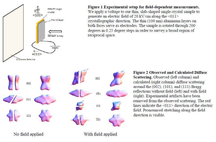
The x-ray diffraction patterns obtained from PZN-PT are interesting because the Bragg peaks are not sharp bright spots as would normally be expected from a perfect crystalline material, rather the peaks are surrounded by highly structured regions of diffuse x-ray scattering. In other words, the Bragg peaks are “smeared out” and take on a unique and interesting three-dimensional shape in reciprocal space, or the mathematical space where x-ray diffraction is most naturally understood. Furthermore, these three-dimensional regions of diffuse scattering, sometimes called “butterflies” because of their structure2 (see Fig. 2), change markedly when a strong electric field is applied to the crystal. The presence of the butterflies and the evolution of their shape when an electric field is applied provide clues into the behavior of the atoms in the material on a sub-nanometer scale. My role has been to plan, prepare, and conduct electric field dependent diffuse scattering measurements at the Advanced Photon Source synchrotron of Argonne National Laboratory in Lemont, IL, and then to analyze our results, together with the results of a previous diffuse scattering experiment without the electric field, to develop and fit a mathematical and physical model to the data.
Significant care and planning were required to enable us to successfully and safely apply an in-situ electric field to our crystal samples of PZN-PT while taking diffuse scattering measurements. I fashioned each sample into a slab of dimensions 3mm x 3mm x 0.3mm, oriented such that a relevant crystallographic direction was normal to the large flat faces. This required extensive use of the x-ray diffractometer at BYU. For purposes of this study, we used the sample with the crystallographic direction as the normal to the face. Using thermal evaporation techniques, I deposited 100 nm of aluminum onto each face and connected small leads to allow us to apply an electric field of magnitude 20 kV/cm along the direction. Once at the beamline at the Advanced Photon Source, we were able to mount our samples and commence the data collection. To survey a broad region of reciprocal space at high resolution, we rotated the crystal through 200 degrees and took exposures in .25-degree steps. The intensity count of each pixel was stored as a 32-bit floating point value in a TIFF file. Figure 1 illustrates this setup.
Since the reciprocal space position represented by each pixel on the detector can be calculated for each exposure, it is possible to extract intensity data for three-dimensional regions of reciprocal space. We employed a rebinning process to reconstruct high-resolution volumes of reciprocal space in three dimensions, thereby allowing us to quantitatively investigate diffuse scattering features. For each Bragg peak in the volume of reciprocal space surveyed by our 200-degree runs, we were able to recreate the surrounding regions of diffuse scattering. It was immediately apparent that the effect of the electric field was to stretch the diffuse scattering in the direction of the field and suppress the scattering perpendicular to the field (Fig.2). We were then able to use these reconstructions of reciprocal space to quantitatively evaluate our mathematical model.
Based on previous work done by my mentor, we were able to identify a mathematical model that reproduces with impressive accuracy the diffuse scattering observed without an applied electric field. We are currently preparing a scientific article for submission to Nature Materials, and since this is a highly studied topic, I am not at liberty reveal the details of the model at this point. In essence, it is based on simple physical properties of the material, offering an appealingly elegant explanation for the zero field diffuse scattering. This was an exciting discovery, but it soon became clear that the model as it stood was not capable of reproducing the diffuse scattering observed in the presence of an applied electric field. After some further investigation, however, I discovered that the inclusion of one additional free parameter in the model caused exactly the type of stretching observed in the diffuse scattering with an applied electric field. This is an extremely interesting result with equally interesting physical implications, as will be discussed in our publication. Thus, with a surprisingly simple model, we are able to calculate with excellent accuracy the diffuse scattering observed in PZN-PT both with and without an applied electric field. Our work constitutes the first quantitative model based on physical properties of the crystal to successfully reproduce the unique diffuse scattering features in PZN-PT. It represents significant progress in the current understanding of PZNPT and the mechanisms by which it demonstrates such impressive and technologically useful properties.
References
- Z. Kutnjak, J. Petzelt, and R. Blinc, Nature 441 (2006).
- H. Hiraka, S. H. Lee, P. M. Gehring, G. Y. Xu, and G. Shirane, Phys Rev B 70, 184105 (2004).
Figures